Articles :-
Buffer amplifier
A buffer amplifier, or simply a buffer, is an electronic amplifier that is designed to have an amplifier gain of 1. Buffers are used in Impedance matching, the benefit of which is to maximize energy transfer between circuits or systems.
There are two main kinds of buffer circuits, Voltage buffers and Current buffers. The purposes of each is to isolate the mentioned characteristic to avoid loading the input circuit or source from the output stage.
Another name by which buffer amplifiers are known as is a voltage follower. The name is given because of the characteristic of the amplifier to output a signal of the same amplitude as the input (given the unity gain [gain of 1 or 0dB] ).
Examples of Buffer amplifiers:
The examples are too many to mention in this page, the most common being the transistor voltage follower and op amp version of it. The exact characteristics, formulas and construction instructions can be found on the specific component's page.
Amplifier Gain
This is one the main characteristics to determine when designing or choosing an amplifier. This is a measure of the increase (or decrease in case of negative gain) the amplitude of the input signal.
Representation:
There are a few different ways to represent amplifier gain. One of the more common way among beginners and hobbyists, specially for DC or small signals, is to describe gain as the ratio of input vs output amplitude:
Gain = Vout/Vin, Where both input and output are either voltage or current (amperage).
Another way to represent amplifier gain is using a logarithmic decibel scale (dB). This representation is calculated using the ratio of input/output powers using the formula:
Gain = 10log(Pout/Pin)
Utility of gain:
There are countless applications and uses for amplifiers, since in the electronics world most signals we get from sensors or transmission lines is very small. There are also other times when not the amplitude of the signal is required but its power to transform into useful work, like when powering a motor, transmitting a radio signal and displaying an image on a screen.
How to calculate:
The specifics of how much gain can an amplifier have depend heavily on the components or circuits used, as well as the topology (configuration) of the amplifier. You can have a better understanding of the formulas used for each component and configuration by going to the specific page.
Amplifiers
Amplifiers increase either the amplitude (voltage) or power (Amperage/Current)
applied to its input.
Components of an amplifier:
Gain component: The main component of the amplifier, defines many of its characteristics like noise, bandwidth, gain, input and output impedance, and others.
Bias: Some types of components need a bias point in order to operate correctly. The bias point is a dc voltage applied to the input of the amplifier. There are many ways to set the bias point,
depending on the gain component used.
Accessories: These are many kinds of sub-circuits used to fine tune the operation of the amplifier, including preamplifiers, buffers, stabilizers, filters, limiters, etc..
Stages of Amplifiers:
Input: This stage consists of a signal from another subsystem outside the amplifier, or a sensor like a microphone, photodiode or any other component that delivers a small signal. Depending on
the intended purpose and input signal, this stage may contain a preamplifier, which is a signal (voltage) amplification before the main power (current) amplification stage, and a filter to
limit incoming frequencies.
Amplification: Main stage of any amplifier, most of the times it is a power amplification process, sometimes with signal amplification as well. This stage is where the gain component and many of the accessories like stabilizers and limiters are located.
Output: Last stage, sometimes consists of a buffer and/or filter to remove any noise generated in the main amplification stage. The buffer sometimes added to deliver more current (lower output impedance).

Block Diagram of a Amplifiers
(Click to enlarge)
Description of Amplifier accessories:
Coupling: This is usually done with a capacitor. The purpose of the coupling capacitor is to prevent any DC voltage from modifying the bias point of the amplifier, to prevent clipping (driving the signal to the max voltage, distorting it) from a high or low bias point.
Another coupling method is using transformers. This is done on lower frequency signals where the reactance (resistance-like behavior when a component is applied an AC voltage) of capacitors is so high to the point the signal is practically lost.
A third choice is using tuned transformers, by using a capacitor in parallel with the transformer. This creates a tuned circuit that has a very narrow bandwidth, useful in some special interest amplifiers.
Filters: This topic is so extensive it deserves its own article. Amplifiers have uses for filters to limit noise and reject unwanted signals from its input. Combining a filter and an amplifier creates an active filter (filter that has gain).
Most filters use RC networks to create the filter, although RL or RLC are also used in some designs.
Stabilizers: This is usually some kind of feedback used to prevent clipping or other circuitry to keep the frequency within a certain range (stop frequency drifting).
Limiters: Sometimes only voltages up to a certain point are needed or desired, here limiters come into use. They limit or sometimes clip a signal if it goes above a certain voltage, other kind of limiters use feedback to control the gain of the amplifier so as to keep the output signal within the specified voltage range.
Buffers: Also called voltage followers, this is just another name for another stage of amplification with a gain of 1. This is to provide more current and avoid overloading the main amplifier, as doing so can reduce either the gain or bandwidth.
If you need a specific implementation of an amplifier circuit, you may want to consider learning all the abstract theory first and then moving on to the components page, where all component-specific circuits and modes of operation are listed.
Types of circuits
From the smallest circuit to the largest electronics project, every circuit that performs a useful function has one or more of the same building blocks. I’m not talking about electronic components; I’m talking about sub-circuits that have a defined function.
These circuits are divided in digital and analog. In these pages you’ll learn how to design every type of circuit listed, with emphasis on a functionality level, instead of a component level, in order to be able to create any kind of amplifier as required by the project. Here’s the list of them:
Analog
There are transistor and OpAmp amplifiers. In transistor amplifiers there are common source, common base, common collector, there are Darlington amplifiers. Transistor amplifiers are further divided by the kind of transistor used: BJT, N-channel JFET, P-channel JFET, MosFET, Nmos, Pmos, Cmos; Each with its own set of configurations.
On OpAmp there are negative feedback, positive feedback, voltage follower and others.
As you can see there are a million different combinations of amplifier topologies as they are called, way too many to be familiar with all of them.
These circuits are divided in digital and analog. In these pages you’ll learn how to design every type of circuit listed, with emphasis on a functionality level, instead of a component level, in order to be able to create any kind of amplifier as required by the project. Here’s the list of them:
Analog
- Amplifiers
- Filters
- Power sources
- Oscillators
- Rectifiers
- Timers
- Modulators
- Demodulators
- Logic gates
- Counters
- Encoders
- Decoders
- Flip-Flops
- Multiplexers
- Demultiplexers
- Analog to Digital Converter (ADC)
- Digital to Analog Converter (DAC)
- Microcontrollers
- Microprocessors
There are transistor and OpAmp amplifiers. In transistor amplifiers there are common source, common base, common collector, there are Darlington amplifiers. Transistor amplifiers are further divided by the kind of transistor used: BJT, N-channel JFET, P-channel JFET, MosFET, Nmos, Pmos, Cmos; Each with its own set of configurations.
On OpAmp there are negative feedback, positive feedback, voltage follower and others.
As you can see there are a million different combinations of amplifier topologies as they are called, way too many to be familiar with all of them.
Logic Gates
Logic gates are the basic building blocks of digital electronics. These are circuits made out of transistors that perform a a logical operation (see Boolean algebra).
Digital electronics represent data (called bits) with only two states. Since in electronics we work with voltages, these two states are most times represented by a presence or lack of voltage. One (high state) in TTL logic familiy is represented by 5v, zero (low state) is represented by 0v (ground).
There are three basic gates: AND, OR, and NOT (Inverter).
Other common gates are NAND, NOR, XOR, XNOR (Equivalence). These gates are made with combinations of the basic logic gates. Its functions can be represented using a truth table, which lists every combination of inputs (A, B) and the resulting output (Z).
AND gate: two input gate, will output 1 when both inputs are 1. It is a one bit multiplication in Boolean algebra.
OR gate: two input gate, will output 1 when one or both inputs are 1. It is a one bit addition.
NOT gate or Inverter: one input gate, will output 1 when the input is 0 and viceversa.
NAND gate: two input gate, same as AND gate but with a NOT at its output. Will output one as long as both its inputs are NOT 1. if none or one of the inputs is 0 it will output 1.
NOR gate: two input gate, same as OR gate but with a NOT at its output. Will output one as long as none of its inputs are 1. if both inputs are 0 it will output 1.
XOR gate: two input gate, will output 1 when one of its inputs is 1, but not both. This gate is actually a combination of gates, its boolean equation is A'B + AB'.
XNOR gate or Equivalence: two input gate, will output 1 when both its inputs are the same, either 0 or 1. XOR gate with a NOT at its output, its boolean equation is A'B' + AB.
Gate Diagrams:

Building other gates with NAND and NOR:
NAND and NOR gates have a remarkable characteristic, with enough of either one of them and connected in a certain way you can actually recreate the behavior of any other gate. This ability has made them very popular for large scale manufacturing of logic gates, since it is cheaper to build only one kind of device instead of having separate machines to create different logic gates for a single circuit.
Here are the circuit diagrams to create other gates with NAND and NOR.
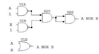
AND gate:

OR gate:

NOT gate:

NAND gate:

NOR gate:
Since all digital electronic circuits are made with transistors, you can make all the above gates using them. When creating logic gates with transistors, the best option is to make them using NAND, NOR and simple NOT gates. The benefit of this is that any other gate can be constructed with a slight variation in the number and configuration of the transistors, instead of having several different circuits for each gate.
Logic gate's transistor diagrams:
NAND gate:


This gate is the simplest one to build with transistors, the NOT gate requires only one transistor. Here the transistor is configured so that when it is on (input 1), the circuit to ground is closed (output 0) and viceversa.
With these schematics and the above diagrams you can create a complete digital circuit using only transistors and resistors. Digital gates are very flexible, but up to a point. When creating a circuit that has more than three or four inputs, the circuit becomes too large to build using only logic gates, and that is where programmable devices come in handy, which we'll discuss in another article.
Digital electronics represent data (called bits) with only two states. Since in electronics we work with voltages, these two states are most times represented by a presence or lack of voltage. One (high state) in TTL logic familiy is represented by 5v, zero (low state) is represented by 0v (ground).
There are three basic gates: AND, OR, and NOT (Inverter).
Other common gates are NAND, NOR, XOR, XNOR (Equivalence). These gates are made with combinations of the basic logic gates. Its functions can be represented using a truth table, which lists every combination of inputs (A, B) and the resulting output (Z).
AND gate: two input gate, will output 1 when both inputs are 1. It is a one bit multiplication in Boolean algebra.
A B | Z
--------
0 0 | 0
0 1 | 0
1 0 | 0
1 1 | 1
--------
0 0 | 0
0 1 | 0
1 0 | 0
1 1 | 1
OR gate: two input gate, will output 1 when one or both inputs are 1. It is a one bit addition.
A B | Z
--------
0 0 | 0
0 1 | 1
1 0 | 1
1 1 | 1
--------
0 0 | 0
0 1 | 1
1 0 | 1
1 1 | 1
NOT gate or Inverter: one input gate, will output 1 when the input is 0 and viceversa.
A | Z
------
0 | 1
1 | 0
------
0 | 1
1 | 0
NAND gate: two input gate, same as AND gate but with a NOT at its output. Will output one as long as both its inputs are NOT 1. if none or one of the inputs is 0 it will output 1.
A B | Z
--------
0 0 | 1
0 1 | 1
1 0 | 1
1 1 | 0
--------
0 0 | 1
0 1 | 1
1 0 | 1
1 1 | 0
NOR gate: two input gate, same as OR gate but with a NOT at its output. Will output one as long as none of its inputs are 1. if both inputs are 0 it will output 1.
A B | Z
--------
0 0 | 1
0 1 | 0
1 0 | 0
1 1 | 0
--------
0 0 | 1
0 1 | 0
1 0 | 0
1 1 | 0
XOR gate: two input gate, will output 1 when one of its inputs is 1, but not both. This gate is actually a combination of gates, its boolean equation is A'B + AB'.
A B | Z
--------
0 0 | 0
0 1 | 1
1 0 | 1
1 1 | 0
--------
0 0 | 0
0 1 | 1
1 0 | 1
1 1 | 0
XNOR gate or Equivalence: two input gate, will output 1 when both its inputs are the same, either 0 or 1. XOR gate with a NOT at its output, its boolean equation is A'B' + AB.
A B | Z
--------
0 0 | 1
0 1 | 0
1 0 | 0
1 1 | 1
--------
0 0 | 1
0 1 | 0
1 0 | 0
1 1 | 1
Gate Diagrams:

Building other gates with NAND and NOR:
NAND and NOR gates have a remarkable characteristic, with enough of either one of them and connected in a certain way you can actually recreate the behavior of any other gate. This ability has made them very popular for large scale manufacturing of logic gates, since it is cheaper to build only one kind of device instead of having separate machines to create different logic gates for a single circuit.
Here are the circuit diagrams to create other gates with NAND and NOR.
AND gate:

OR gate:

NOT gate:

NAND gate:

NOR gate:

Since all digital electronic circuits are made with transistors, you can make all the above gates using them. When creating logic gates with transistors, the best option is to make them using NAND, NOR and simple NOT gates. The benefit of this is that any other gate can be constructed with a slight variation in the number and configuration of the transistors, instead of having several different circuits for each gate.
Logic gate's transistor diagrams:
NAND gate:

For this gate, the transistors are connected in series, so that the path from the output to ground is completed (thus giving 0 as output) only when both transistors are on (both inputs 1)
NOR gate:
For the NOR gate, the transistors are connected in parallel, so that the circuit from the output to ground is closed when either transistor is on.
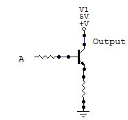
NOT gate:
This gate is the simplest one to build with transistors, the NOT gate requires only one transistor. Here the transistor is configured so that when it is on (input 1), the circuit to ground is closed (output 0) and viceversa.
******Related Topics *****
Electronics Lab Created By Muhammad Irfan


very nice article
ReplyDelete