Saturday, November 30, 2013

3V to 9V DC Converters

1 comment:
Here are some 3V to 9V DC converter circuits that were requested by some of our visitors. It may be helpful to have one of this converters when no 9V battery is available or if you consider that they are too expensive. The first circuit is very simple, it uses the TL496 power supply controller, a coil and a electrolytic capacitor.


TL496 3 to 9 volt converter circuit
tl496 3 to 9V dc converter
The maximum output voltage is actually 8.6V and current is around 80mA.
The input current (the current drawn from the batteries) is 405mA at the maximum output current. Without load the current consumption is 125µA and the batteries life is around 166 days.


Here is another 1.5… 4.5V to 9V converter


3 volt to 9 volt with LMC555
This dc converter is built with the CMOS version of 555 timer. You can get 12V too if you change the zener diode to a 12V version.
3volt 9volt 555 timer
Probably there are more 3 to 9 volt dc converters but for the moment those are the only ones presented in this article.


******Related Topic ******


-------------------------------------------------------------------------------------------------------------------

1.5V Battery to 5V Voltage Converter

4 comments:

 1.5V Battery to 5V Voltage Converter


Wanna recharge your portable music player through its USB power interface, during a winter trip? Or like to energise a microcontroller based circuit using a single penlight cell? Here is an interesting circuit to generate stable and secure 5V DC (at 200mA max) from an ordinary 1.5V AA sized cell. At the heart of this circuit is IC1 MAX756 from Maxim, which is a CMOS step-up DC-DC switching regulator for small, low input voltage or battery-powered systems.


MAX756 accepts a positive input voltage down to 0.7V and converts it to a higher pin selectable output voltage of 5V (or 3.3V). Typical full-load efficiency for the this IC is greater than 87%. Max756 combine a switch-mode regulator with an N-channel MOSFET, precision voltage reference, and power-fail detector in a single monolithic device. The MOSFET is a “sense-FET” type for best efficiency, and has a very low gate threshold voltage to ensure start-up under low-battery voltage conditions (1.1V typ).
assembled circuit
inductor coilThe circuit can be easily wired on a very small rectangular common PCB.All connections should be kept as short as possible. If available,try to add a good quality 8 pin DIP socket for IC1. Note that the power inductor’s (L1) DC resistance significantly affects efficiency. For highest efficiency, limit L1’s DC resistance to 0.03 Ohm or less. A thru-hole type standard power inductor can be used. Similarly, the ESR of all capacitors (bypass and filter) affects circuit efficiency. Best performance is obtained by using specialized low-ESR capacitors.
5 Volt From 1.5 Volt Circuit Schematic


portable 1.5 V to 5 V converter schematic


Thursday, November 28, 2013

FM remote Encoder/Decoder

No comments:
  FM remote Encoder/Decoder


Description.
Here is the circuit diagram of an FM remote encoder/decoder using the ICs RF600E and RF600D. These devices are designed to provide a high level of security and operates from anything between 2 to 6.6V DC. Various electronic circuits like remote control systems, remote alarm systems, anti theft alarms etc can be implemented using the RF600E/RF600D pair.
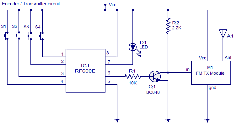
The remote systems given here uses FM for the transmission. IC1 RF600E and its associated components form the encoder circuit. Pins 1 to 4 forms the switch inputs of IC1. When each push button switch is pressed a corresponding code will be generated at the pin 6 which is the data output pin. The encoded signal available at pin 6 is buffered using the transistor Q1 and the fed to the input of a general purpose FM transmitter module (M1). Such FM transmitter modules are very common in the market now.
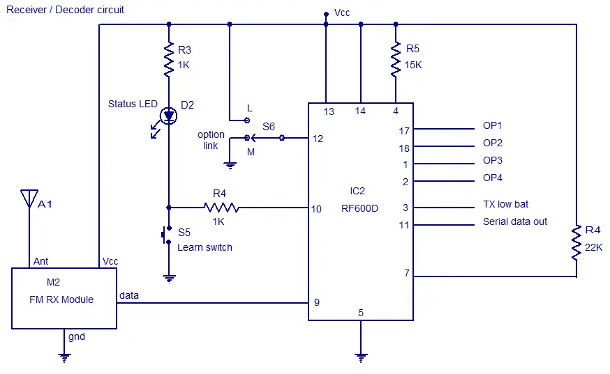
The decoder system comprises of the IC2 RF600D and its associated components. Pins 17, 18, 1 and 2 are the digital data output pins of RF600D corresponding to the input switches S1 to S4 of the encoder/transmitter circuits. The digital data output pins 17,18,1 and 2 are asserted low when the relevant inputs S1 to S4 on the IC2 RF600E are asserted. M2 is a general purpose FM receiver module which receives the transmitted code and feds it to the data input (pin 9) of the IC2. Switch S1 can be used to select between latching and momentary digital output function. In latching mode digital output pins (OP1 to OP4) are only asserted for the corresponding transmit signal. In latching mode the output state is changed on each corresponding transmit signal. The learn switch S5 is used to enter the decoder IC in to the “learn mode”. Learn operation using push button switch S5 is as follows. 1) Press and release the push button switch S5. 2) The status LED D2 will glow when S5 is pressed and will remain ON when S5 is released. 3) Operate the encoder/transmitter once. 4) The status LED D2 will become OFF. 5) Operate the encoder/transmitter again. 6) The status LED will start flashing. 7) When the flashing of status LED stops, the encoder will be successfully taught to the decoder and the transmitter/encoder will now operate the receiver/decoder system. Up to seven encoder/transmitters can be learnt to each RF600D.Pin 3 of IC2 is the transmitter low battery indicator output and pin 11 is the serial data output.


Circuit diagram.


FM remote encoder circuit 


FM remote decoder circuit


Notes.
  • Assemble the circuit on a good quality PCB.
  • The ICs can be operated from anything between 2V to 6.6V.
  • Switches S1 to S5 are miniature push button switches.
  • S6 can be a miniature two way switch.
  • Transmit LED D1 will glow whenever the encoder is transmitting.
  • The power supply must be properly regulated and ripple free.
  • I recommend using batteries for powering the circuit.
  • Go through the datasheets of RF600E and RF600D before attempting this circuit.

5 channel radio remote control

No comments:

TX-2B / RX / 2B  5 channel radio remote control.

This article is about a simple 5 channel radio remote control circuit based on ICs TX-2B and RX-2B from Silan Semiconductors. TX-2B / RX-2B is a remote encoder decoder pair that can be used for remote control applications. TX-2B / RX-2B has five channels, wide operating voltage range (from 1.5V to 5V), low stand by current (around 10uA), low operating current (2mA), auto power off function and requires few external components. The TX-2B / RX-2B was originally designed for remote toy car applications, but they can be used for any kind of remote switching application.

Circuit diagrams and description.

Remote encoder / transmitter circuit.

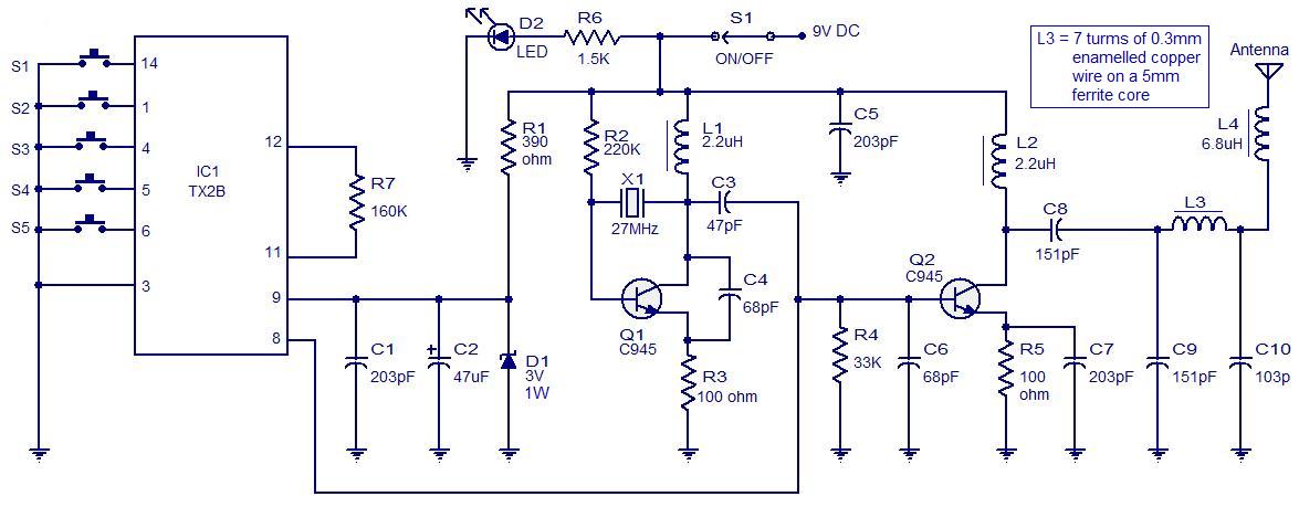
radio remote control transmitter ciruit
5 channel redio remote control encoder / transmitter circuit
The TX-2B forms the main part of the circuit. Push button switches S1 to S5 are used for activating (ON/OFF) the corresponding O/P channels in the receiver / decoder circuit. These push button switches are interfaced to the built-in latch circuitry of the TX-2B. Resistor R7 sets the frequency of the TX-2B’s internal oscillator. Resistor R1 and Zener diode D1 forms a simple Zener regulator circuit for providing the IC with 3V from the 9V main supply. C2 is the filter capacitor while C1 is a noise by-pass capacitor. D2 is the power on indicator LED while R6 limits the current through the same LED. S1 is the ON/OFF switch. The encoded control signal will be available at pin 8 of the IC. The encoded signal available at pin 8 is without carrier frequency. This signal is fed to the next stage of the circuit which is a radio transmitter. Crystal X1 sets the oscillator frequency of the transmitter section. R2 is the biasing resistor for Q1 while R3 limits the collector current of Q1. The encoded signal is coupled to the collector of Q1 through C3 for modulation. Transistor Q2 and associated components provide further amplification to the modulated signal.

Remote receiver / decoder circuit.

5 channel radio remote decoder

The remote receiver circuit is built around the IC RX-2B. The first part of the circuit is a radio receiver built around transistor Q1. The received signal is demodulated and fed to pin 14 of the IC. Pin 14 is the input of the built in inverter inside the IC. R2 sets the frequency of the IC’s internal oscillator. O/P 1 to O/5 are the output pins that are activated corresponding to the push buttons S1 to S5. Zener diode D1 and resistor R12 forms an elementary Zener regulator for supplying the RX-2B with 3V from the 9V main supply. C12 is the filter capacitor while R11 is the current limiter for the radio receiver section. Diode D2 protects the circuit from accidental polarity reversals. C15 is another filter capacitor and C14 is a noise by-pass capacitor.

Notes.

  • This circuit can be assembled on a vero board or a PCB.
  • Use 9V DC for powering the transmitter / receiver circuits.
  • Battery is the better option for powering the transmitter / receiver circuit.
  • If you are using a DC power supply circuit, it must be well regulated and free from any sort of noise.
  • Both ICs must be mounted on holders.

Interfacing relay to the RX-2B output.

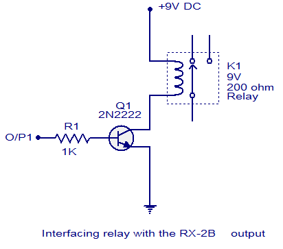
The method for interfacing a relay to the output of RX-2B is shown below. When push button switch S1 of the transmitter circuit is pressed, pin O/P1 (pin 7 of the RX-2B) goes high. This makes the transistor 2N2222 to conduct and the relay is activated. The same technique can be applied to other output pins of the RX-2B. The relay used here is a 200 ohm type and at 9V supply voltage the load current will be 45mA which is fine for 2N2222 whose maximum possible collector current is 900mA. When using relays of other ratings this point has to be remembered and do not use a relay that consumes a current more than the maximum possible collector current of the driver transistor.
transistor relay driver
Interfacing relay to the remote decoder