A bipolar junction transistor (BJT) has three regions, of which the emitter and the collector are made of the same type of semiconductor (‘n’ for npn and ‘p’ for pnp) but the base is of opposite type. If we consider the base and emitter terminals (or the base and collector terminals), we get a p-n junction diode. But if we hold collector and emitter terminals, we encounter two diodes connected back-to-back.
On forward biasing the p-n junction (with a battery and a current-limiting resistor), the diode starts conducting and the drop of voltage across it is very small (0.7 volt for Si). On reverse biasing, the diode stops conducting and the drop of voltage across it is very close to the supply voltage. But, practically no current will flow through the collector and emitter terminals when we make the collector positive with respect to the emitter or vice versa.
This is the basis of the first part of our experiment that helps determine the type of a given transistor (whether npn or pnp) as also its base. But we cannot distinguish between the collector and the emitter in this way. To do so, we have to understand another basic principle.
BJTs have an intrinsic property of current amplification. While operating in the active region, a small current injected into the base can produce a large current flowing between the collector and emitter. The ratio of the collector current to the base current is known as forward current gain βF.
Although the collector and the emitter are made of the same type of semiconductor, we cannot expect a large current gain if we treat the collector as the emitter and the emitter as the collector.
If we forward bias the collector-base junction and reverse bias the base-emitter junction, we call it the inverse mode of operation. Because of the structural difference and doping levels, inverse current gain βI is exceedingly small. Thus while βF can be of the order of hundreds, βI is of the order of a few units only. This principle will be utilised in the second part of our experiment to distinguish between the collector and the emitter leads.
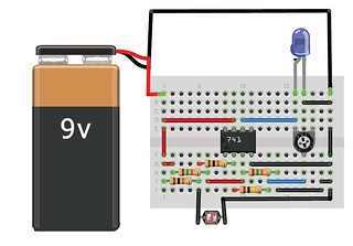
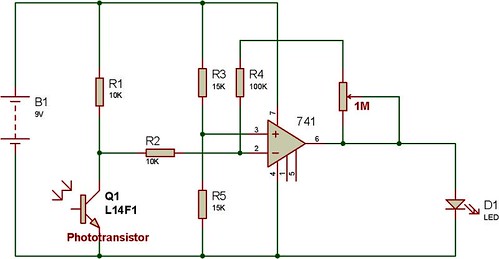
At the heart of the circuit (shown in Fig. 1) is a comparator built around operational amplifier IC 741 (IC1). With the help of a divider network comprising R3 and R4 between the positive supply terminal and ground, the inverting terminal is kept at reference voltage Vref=VssR4/(R3+R4) or –VssR4/(R3+R4) depending upon the selection of contact +Vss (marked ‘npn’) or –Vss (marked ‘npn’) by SPDT switch S1. The voltage at the non-inverting terminal is taken from the bottom end of resistor R2 (1-kilo-ohm) marked V+.
If V+>Vref, the comparator output will be high (positive saturation state ≈ +Vss) and the red LED will glow. On the other hand, if V+<Vref,the comparator output will be low(negative saturation state ≈ –Vss) andthe green LED will glow. The transi-tion from one state to the other is verymuch abrupt and under no circum-stances can both LEDs be ‘on’ or ‘off.’
The first part of the experiment for determination of the transistor type may be carried out as follows:
1. Label the terminals of the transistor under test (TUT) as 1, 2 and 3 arbitrarily.
2. Keeping aside socket C, use only sockets A and B in this part of the experiment.
3. Select the contact marked ‘n-p-n.’ This makes the voltage at socket A positive with respect to socket B (GND).
4. Take any pair of terminals of the transistor and insert one terminal in socket A and the other in socket B. Observe which LED turns on and which remains ‘off’ and record it.
5. Next, interchange the terminals in the two sockets and again observe the status of the LEDs and record it.
6. Repeat steps 4 and 5 for the remaining two pairs and record all the six observations in the form of a table.
From Table I, first find out the pair of terminals for which only the red LED glows even when the terminals are interchanged. These are the collector and emitter terminals. You cannot, however, detect which one of these would be the collector or the emitter from this part of experiment.
Once you have separated the collector and the emitter leads, the remaining lead will obviously be the base of the transistor.
Right up to this point, we do not know whether the transistor is npn- or pnp-type, because the assertion made above will remain valid for the collector and the emitter both being either ‘n’ type or ‘p’ type. The only thing we know is that the base will be of opposite-type semiconductor.
Since we know the polarity of ‘A’ (positive w.r.t. ‘B’), we search from Table I which LED was glowing when the base was put in socket A and any one of the other two leads in socket B.
If the green LED was glowing the base is p-type and the transistor is npn-type, but if the red LED was glowing the base is n-type and the transistor is pnp-type.
A typical record is shown in Table I, from which we find that the transistor is npn-type and lead 2 is the base. But, lead 1 or lead 3 could be the emitter or vice versa.
To detect the collector and the emitter, proceed as follows:
7. If the transistor is npn-type, set the pole of switch S1 towards ‘npn’ marking. If the transistor is pnp-type, set the pole of switch S1 towards ‘pnp’ marking.
8. Next, insert the base lead in socket C, any one of the remaining two leads in socket A and the rest in socket B. Observe as before the status of the two LEDs.
For an npn-type transistor, if the green LED glows the lead inserted in socket A will be collector, but if the red LED glows it will be emitter.
On the other hand, for a pnp-type transistor, if the green LED glows the lead inserted in socket A will be emitter, but if the red LED glows the reverse will be the case, i.e., the lead will be collector.
The status of the LEDs for the above-mentioned npn-type transistor having lead 2 as base is shown in Table II. From this table, we find that lead 1 is collector and lead 3 is emitter of the transistor in the example.
Electronics Lab created by Muhammad Irfan
On forward biasing the p-n junction (with a battery and a current-limiting resistor), the diode starts conducting and the drop of voltage across it is very small (0.7 volt for Si). On reverse biasing, the diode stops conducting and the drop of voltage across it is very close to the supply voltage. But, practically no current will flow through the collector and emitter terminals when we make the collector positive with respect to the emitter or vice versa.
 |
BJTs have an intrinsic property of current amplification. While operating in the active region, a small current injected into the base can produce a large current flowing between the collector and emitter. The ratio of the collector current to the base current is known as forward current gain βF.
Although the collector and the emitter are made of the same type of semiconductor, we cannot expect a large current gain if we treat the collector as the emitter and the emitter as the collector.
If we forward bias the collector-base junction and reverse bias the base-emitter junction, we call it the inverse mode of operation. Because of the structural difference and doping levels, inverse current gain βI is exceedingly small. Thus while βF can be of the order of hundreds, βI is of the order of a few units only. This principle will be utilised in the second part of our experiment to distinguish between the collector and the emitter leads.
At the heart of the circuit (shown in Fig. 1) is a comparator built around operational amplifier IC 741 (IC1). With the help of a divider network comprising R3 and R4 between the positive supply terminal and ground, the inverting terminal is kept at reference voltage Vref=VssR4/(R3+R4) or –VssR4/(R3+R4) depending upon the selection of contact +Vss (marked ‘npn’) or –Vss (marked ‘npn’) by SPDT switch S1. The voltage at the non-inverting terminal is taken from the bottom end of resistor R2 (1-kilo-ohm) marked V+.
 |
1. Label the terminals of the transistor under test (TUT) as 1, 2 and 3 arbitrarily.
2. Keeping aside socket C, use only sockets A and B in this part of the experiment.
3. Select the contact marked ‘n-p-n.’ This makes the voltage at socket A positive with respect to socket B (GND).
4. Take any pair of terminals of the transistor and insert one terminal in socket A and the other in socket B. Observe which LED turns on and which remains ‘off’ and record it.
5. Next, interchange the terminals in the two sockets and again observe the status of the LEDs and record it.
6. Repeat steps 4 and 5 for the remaining two pairs and record all the six observations in the form of a table.
From Table I, first find out the pair of terminals for which only the red LED glows even when the terminals are interchanged. These are the collector and emitter terminals. You cannot, however, detect which one of these would be the collector or the emitter from this part of experiment.
Once you have separated the collector and the emitter leads, the remaining lead will obviously be the base of the transistor.
 |
Since we know the polarity of ‘A’ (positive w.r.t. ‘B’), we search from Table I which LED was glowing when the base was put in socket A and any one of the other two leads in socket B.
If the green LED was glowing the base is p-type and the transistor is npn-type, but if the red LED was glowing the base is n-type and the transistor is pnp-type.
A typical record is shown in Table I, from which we find that the transistor is npn-type and lead 2 is the base. But, lead 1 or lead 3 could be the emitter or vice versa.
To detect the collector and the emitter, proceed as follows:
7. If the transistor is npn-type, set the pole of switch S1 towards ‘npn’ marking. If the transistor is pnp-type, set the pole of switch S1 towards ‘pnp’ marking.
8. Next, insert the base lead in socket C, any one of the remaining two leads in socket A and the rest in socket B. Observe as before the status of the two LEDs.
For an npn-type transistor, if the green LED glows the lead inserted in socket A will be collector, but if the red LED glows it will be emitter.
On the other hand, for a pnp-type transistor, if the green LED glows the lead inserted in socket A will be emitter, but if the red LED glows the reverse will be the case, i.e., the lead will be collector.
The status of the LEDs for the above-mentioned npn-type transistor having lead 2 as base is shown in Table II. From this table, we find that lead 1 is collector and lead 3 is emitter of the transistor in the example.
Electronics Lab created by Muhammad Irfan