Thursday, December 26, 2013

8051 Programming Tutorial

No comments:

8051 Programming Tutorial


This article series is developed to teach you 8051 micro controller programming. I have divided this programming tutorial into a series of chapters as shown below. So you can start with Chapter 1 and then move to chapter 2 and chapter 3 and so on. So let’s begin the journey right now! 
Note: Next chapters 1,2,3.. are under development phase. Please visit this page again for updates.
Note: To test any of these program or to write one your own and test, you dont need to buy a microcontroller board now. You can test your program using an 8051 simulator. Here is a big list of 8051 simulators available. In the beginning try the first one given in the list, Edsim51. Its an easy to use tool. 
To program any microcontroller available in this world, first you need to learn and understand it’s instruction sets. Instruction set contains a set of instructions that is available for the programmer to create any kind of program he likes. Or in another way, using the instruction set a programmer can create the program required for the specific application he is making. So first of all one needs to master all available instructions, how an instruction works, how the execution of an instruction affects the microcontroller (affecting the registers, psw, stack etc) and the way it is used in a program. Once the instruction set is mastered, you can start playing with programs. Before getting into programming, there are some prerequisites. If you are really new to micro controller and if 8051 is the first one you are playing with, please read the following articles first.
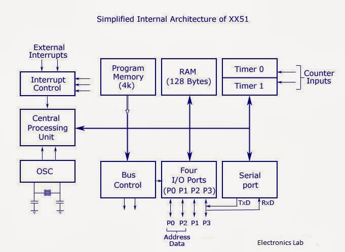
1. Difference between Microprocessor and Micro controller
2. Basics of 8051 Microcontroller – Pin diagram – Architecture – Memory Organization
3. Addressing modes of 8051 You must read this article before writing any program for 8051 as this documents the root of instruction handling.
4.  8051 Special Function Registers and I/O Ports
Now lets come to instruction sets of 8051 micro controller.  The 8051 instruction set can be classified as shown below.
  • Instructions for data transfer/ data move
  • Instructions for arithmetic operations
  • Instructions for branching a program
  • Instruction for creating subroutines
  • Instructions for logical operations
  • Instructions for boolean operations 
  • Special purpose instructions
Follow the given link, where you can access the complete list of instructions for 8051 micro controller – 8051 Instruction Set  (see the heading Alphabetical order below first table).
Note:- 8051 micro controller belongs to the MCS-51 family of micro controllers.  This basically means,any 8051 variant micro controller (that comes under the MCS-51 family) made by any other manufacturer must use the same set of instructions made for MCS-51. So the “instruction decoder” part of all micro controllers under MCS-51 family is same. Example: Atmels AT89c2051 is one such micro controller that falls under MCS-51 family. So a program written for Intel 8051 can be used to run AT89C2051 too (you may have to make slight modifications to match hardware disparities).

1. Instructions for data transfer includes – MOV, MOVC, MOVX, PUSH, POP, XCH, XCHD
2.Instructions for arithmetic operations are – ADD, ADDC, SUBB, MUL, DIV, INC, DEC, DA A
3. Instructions for branching and subroutines – LJMP, AJMP, SJMP, LCALL, ACALL, JZ, JNZ, CJNE, DJNZ, JMP, NOP, RET, RETI
4. Instructions for logical operations – ANL, ORL, XRL, CLR, CPL, RL, RLC, RR, RRC, SWAP
5. Instructions for boolean variable operations – SETB, MOV, CLR, JB, JNB, JBC, ANL, ORL, CPL, JC, JNC
6. Special purpose instructions involves – MOVC, MOVX, SWAP, XCH, XCHD, JBC, RETI, DA A
You may learn about all instructions in detail by following that link given above. There are 44 instructions in 8051 or MCS-51 instruction set.
I assume you have gone through data transfer/arithmetic/branching and subroutine instructions by now. Now lets write a very simple program.

A program to find sum of N natural numbers and store the sum


Program description:-

  The number “N” is stored in location 35H. Natural numbers generated from 0 to N must be stored from location 55H. The sum of natural numbers must be stored in location 36H.
Analyzing the program description, we need 3 registers. R0 to store the value of “N”  (given in location 35H)and to act as a counter for generating natural numbers upto N. R5 is used to save the value of first storage location of natural numbers and then R5 is incremented by one each to store each newly generated natural number. R7 is initiated as 0 and is incremented by 1 to generate natural numbers.

The Program:-

MOV PSW, #00H // Register bank '0' is selected by executing this instruction.
MOV R0, 35H // The value of 'N' stored in location 35H is transfered to R0.
MOV R5, #55H// The starting location for storing natural numbers '#55H' is transfered to R5
MOV A, #00H// Accumulator is initiated with value 0 for adding natural numbers cumulatively.
MOV R7, #00H// R7 is initialized to '0' to generate natural numbers. Note: '0' is not a natural number.
LOOP: INC R7// R7 is incremented by 1 to generate next natural number.
MOV @R5, 07H// This is indirect addressing mode used here.It is not possible to transfer data from one register to another register directly. So an instruction like MOV R5, R7 is invalid.Instead we use the direct address (07) of register R7 of register bank #00 to transfer the generated natural number to it's storage location in register R5.Indirect addressing is used as we need to save the generated natural number directly to memory address. R5 holds the starting location address (of the storage area) as its value i.e #55H.By indirectly addressing, we can save what ever value in R7 directly to location #55H.
INC R5// The storage location is incremented by 1 from #55H to #56H to store the next generated natural number
ADD A, R7// The generated natural number is added to contents in accumulator.
DJNZ R0, LOOP// The value of register Ro (value of 'N') is decremented by 1. It is checked against stopping condition zero. If its R0 is not equal to zero, the program control will move to label LOOP again and the steps from INC R7 will be executed again until R0 is equal to zero. When R0 is equal to zero, program control will exit the loop and move to next instruction given below.
MOV 36H,A// The sum of natural numbers in accumulator is moved to storage location 36H.
STOP: SJMP STOP// An infinite loop written at the end of the program. When this instruction is reached program control will get stuck at this instruction as it's an infinite loop.To get out of this infinite loop system reset must be applied.


A simple program to copy a block of data from one location to another

Program Description:-

10 bytes of data stored from 30H is to be copied to another location staring from 50H.
Analyzing the program, we see, we need two registers to store starting locations of source and destination. Lets say we take R0 as the source and R2 as the destination registers. Now we need a counter to count 10 bytes of data transfered from source to destination. Lets take R3 for that. It is not possible to transfer data from one register to another register directly by using any kind of addressing mode. So we need accumulator to stand in between as a temporary register. So here is it:

The Program:

MOV R0,#30H // Address of the starting location of source data is moved to R0.
MOV R1,#50H // Address of the starting location of destination is moved to R1
MOV R3,#OAH// Set the counter R3 with 10. You can also use decimal number as MOV R3,#10d.
LOOP: MOV A, @R0// Indirect addressing mode is used. Contents at the location of Ro (30H) is copied to accumulator.
MOV @R1, A// Contents in accumulator is copied to location pointed by Ra (that is 50H).
INC R0 // Ro is incremented by 1 to point to next location.
INC R1// R1 is incremented by 1 to point to next location.
DJNZ R3, LOOP // Counter register R3 is decremented by 1 and checked against zero. See the explanation DJNZ in the first program "sum of natural numbers"
STOP: SJMP STOP // Infinite loop to terminate programh


The Program:- 

BEGIN: MOV R1,30H // Getting the value of "N"
MOV R7,#40H // The first number '0' of series is stored here.
MOV @R7,#00H // Loading value 'o' to address 40H using indirect addressing
INC R7 // Incrementing value of R7 from 40H to 41H to store next number '1'
MOV @R7, #01H // Storing value '1' to location 41H. Note that 'o' and '1' are seed values of a fibonacci series and has to be generated manually.
MOV R5,#42H // New register R5 is loaded with location address 42H to store next values of series, generated by adding the 2 previously generated numbers.
DEC R1
DEC R1 // The count value "N" is decremented by 2, as we have already generated and stored 1st two numbers.
DEC R7 // R7 is now reduced from 41H to 40H. We need to add contents of 40H and 41 H to get the number that is to be stored in 42H.
LOOP: MOV A, @R7 // Contents in R7 is moved to accumulator.
INC R7 // R7 is incremented to get the next value.
ADD A,@R7 // The two values are added and stored in Acc.
MOV @R5,A // The newly generated value of the series is stored in the address held by R5.
INC R5 // R5 is incremented to store next value.
DJNZ R1,LOOP // The count "N" is checked to zero (to know if all the numbers upto N are generated).
STOP: SJMP STOP // Run infinitely here or end of program execution. 


 These 3 programs will be enough for a “kick start” in 8051 programming. More programs and concepts will be explained in upcoming articles. I recommend you to download Edsim51 simulator (or any other one you prefer) and try out these programs. Make changes to these codes and write simple codes based on your ideas – like Multiplying 2 numbers, Generating a particular series, Arithmetic calculator etc. Only by doing yourself, you can master the art of programming!

Electronics Lab Created By Muhammad Irfan
 

8051 Microcontroller/8051 Microcontroller Architecture

No comments:

8051 Microcontroller/8051 Microcontroller Architecture

A micro controller is an integrated circuit or a chip with a processor and other support devices like program memory, data memory, I/O ports, serial communication interface etc integrated together. Unlike a microprocessor (ex: Intel 8085), a microcontroller does not require any external interfacing of support devices. Intel 8051 is the most popular microcontroller ever produced in the world market. Now lets talk about 8051 microcontroller in detail.
Before going further, it will be interesting for you to understand the difference between a Microprocessor and Microcontroller. We have a detailed article which describes the basic difference between both.


Here is a Quick Access to various sections of this article:-


Introduction

Intel first produced a microcontroller in 1976 under the name MCS-48, which was an 8 bit microcontroller. Later in 1980 they released a further improved version (which is also 8 bit), under the name MCS-51. The most popular microcontroller 8051 belongs to the MCS-51 family of microcontrollers by Intel. Following the success of 8051, many other semiconductor manufacturers released microcontrollers under their own brand name but using the MCS-51 core. Global companies and giants in semiconductor industry like Microchip, Zilog, Atmel, Philips, Siemens released products under their brand name. The specialty was  that all these devices could be programmed using the same MCS-51 instruction sets. They basically differed in support device configurations like improved memory, presence of an ADC or DAC etc. Intel then released its first 16 bit microcontroller in 1982, under name MCS-96

8051 Microcontroller Packaging

There is no need of explaining what each package means, you already know it. So I will skim through mainly used packaging for 8051. See, availability of various packages change from device to device. The most commonly used is Dual Inline Package (40 pins) – known popularly as DIP. 8051 is also available in QFP (Quad Flat Package), TQFP (Thin Quad Flat Package), PQFP (Plastic Quad Flat Package) etc. For explaining the pin diagram, we have used a 40 pin DIP IC as model.

8051 Microcontroller Architecture

Its possible to explain microcontroller architecture to a great detail, but we are limiting scope of this article to internal architecture, pin configuration, program memory and data memory organization. The basic architecture remains same for the MCS-51 family. In general all microcontrollers in MCS- 51 family are represented by XX51, where XX can take values like 80, 89 etc.

Schematic and Features


8051 Microcontroller


A micro controller is an integrated circuit or a chip with a processor and other support devices like program memory, data memory, I/O ports, serial communication interface etc integrated together. Unlike a microprocessor (ex: Intel 8085), a microcontroller does not require any external interfacing of support devices. Intel 8051 is the most popular microcontroller ever produced in the world market. Now lets talk about 8051 microcontroller in detail.
Before going further, it will be interesting for you to understand the difference between a Microprocessor and Microcontroller. We have a detailed article which describes the basic difference between both.
Microprocessor vs Microcontroller 

Here is a Quick Access to various sections of this article:-

Pin Diagram :-  Internal Architecture  :-  Program Memory Organization  :- Data Memory Organization :-8051 System Clock  :- 8051 Reset Circuit

Introduction

Intel first produced a microcontroller in 1976 under the name MCS-48, which was an 8 bit microcontroller. Later in 1980 they released a further improved version (which is also 8 bit), under the name MCS-51. The most popular microcontroller 8051 belongs to the MCS-51 family of microcontrollers by Intel. Following the success of 8051, many other semiconductor manufacturers released microcontrollers under their own brand name but using the MCS-51 core. Global companies and giants in semiconductor industry like Microchip, Zilog, Atmel, Philips, Siemens released products under their brand name. The specialty was  that all these devices could be programmed using the same MCS-51 instruction sets. They basically differed in support device configurations like improved memory, presence of an ADC or DAC etc. Intel then released its first 16 bit microcontroller in 1982, under name MCS-96

8051 Microcontroller Packaging

There is no need of explaining what each package means, you already know it. So I will skim through mainly used packaging for 8051. See, availability of various packages change from device to device. The most commonly used is Dual Inline Package (40 pins) – known popularly as DIP. 8051 is also available in QFP (Quad Flat Package), TQFP (Thin Quad Flat Package), PQFP (Plastic Quad Flat Package) etc. For explaining the pin diagram, we have used a 40 pin DIP IC as model.

8051 Microcontroller Architecture

Its possible to explain microcontroller architecture to a great detail, but we are limiting scope of this article to internal architecture, pin configuration, program memory and data memory organization. The basic architecture remains same for the MCS-51 family. In general all microcontrollers in MCS- 51 family are represented by XX51, where XX can take values like 80, 89 etc.

Schematic and Features


The general schematic diagram of 8051 microcontroller is shown above. We can see 3 system inputs, 3 control signals and 4 ports (for external interfacing). A Vcc power supply and ground is also shown. Now lets explain and go through each in detail. System inputs are necessary to make the micro controller functional. So the first and most important of this is power, marked as Vcc with a GND  (ground potential). Without proper power supply, no electronic system would work. XTAL 1 and XTAL 2 are for the system clock inputs from crystal clock circuit. RESET input is required to initialize microcontroller to default/desired values and to make a new start.
There are 3 control signals, EA,PSEN and ALE. These signals known as External Access (EA), Program Store Enable (PSEN), and Address Latch Enable (ALE) are used for external memory interfacing.
Take a look at the schematic diagram below (a functional microcontroller)


As mentioned above, control signals are used for external memory interfacing. If  there is no requirement of external memory interfacing then, EA pin is pulled high (connected to Vcc) and two others PSEN and ALE are left alone. You can also see a 0.1 micro farad decoupling capacitor connected to Vcc (to avoid HF oscillations at input).
There are four ports numbered 0,1,2,3 and called as Port 0, Port 1, Port 2 and Port 3 which are used for external interfacing of devices like DAC, ADC, 7 segment display, LED etc. Each port has 8 I/O lines and they all are bit programmable.

8051 Pin Diagram & Description


For describing pin diagram and pin configuration of 8051, we are taking into consideration a 40 pin DIP (Dual inline package). Now lets go through pin configuration in detail.
Pin-40 : Named as Vcc is the main power source. Usually its +5V DC.
You may note some pins are designated with two signals (shown in brackets).
Pins 32-39: Known as Port 0 (P0.0 to P0.7) – In addition to serving as I/O port, lower order address and data bus signals are multiplexed with this port (to serve the purpose of external memory interfacing). This is a bi directional I/O port (the only one in 8051) and external pull up resistors are required to function this port as I/O.
Pin-31:- ALE aka Address Latch Enable is used to demultiplex the address-data signal of port 0 (for external memory interfacing.)  2 ALE pulses are available for each machine cycle.
Pin-30:- EA/ External Access input is used to enable or disallow external memory interfacing. If there is no external memory requirement, this pin is pulled high by connecting it to Vcc.
Pin- 29:- PSEN or Program Store Enable is used to read signal from external program memory.
Pins- 21-28:- Known as Port 2 (P 2.0 to P 2.7) – in addition to serving as I/O port, higher order address bus signals are multiplexed with this quasi bi directional port.
Pin 20:- Named as Vss – it represents ground (0 V) connection.
Pins 18 and 19:- Used for interfacing an external crystal to provide system clock.
Pins 10 – 17:- Known as Port 3. This port also serves some other functions like interrupts, timer input, control signals for external memory interfacing RD and WR , serial communication signals RxD and TxD etc. This is a quasi bi directional port with internal pull up.
Pin 9:- As explained before RESET pin is used to set the 8051 microcontroller to its initial values, while the microcontroller is working or at the initial start of application. The RESET pin must be set high for 2 machine cycles.
Pins 1 – 8:- Known as Port 1. Unlike other ports, this port does not serve any other functions. Port 1 is an internally pulled up, quasi bi directional I/O port.


8051 Internal Architecture


There is no need of any detailed explanation to understand internal architecture of 8051 micro controller. Just look at the diagram above and you observer it carefully. The system bus connects all the support devices with the central processing unit. 8051 system bus composes of an 8 bit data bus and a 16 bit address bus and bus control signals. From the figure you can understand that all other devices like program memory, ports, data memory, serial interface, interrupt control, timers, and the central processing unit are all interfaced together through the system bus. RxD and TxD (serial port input and output) are interfaced with port 3.

8051 Memory Organization

Before going deep into the memory architecture of 8051, lets talk a little bit about two variations available for the same. They are Princeton architecture and Harvard architecture. Princeton architecture treats address memory and data memory as a single unit (does not distinguish between two) where as Harvard architecture treats program memory and data memory as separate entities. Thus Harvard architecture demands address, data and control bus for accessing them separately where as Princeton architecture does not demand any such separate bus.
Example:- 8051 micro controller is based on Harvard architecture and 8085 micro processor is based on Princeton architecture.
Thus 8051 has two memories :- Program memory and Data memory

Program memory organization


Now lets dive into the program memory organization 0f 8051. It has an internal program of 4K size and if needed an external memory can be added (by interfacing ) of size 60K maximum. So in total 64K size memory is available for 8051 micro controller.  By default, the External Access (EA) pin should be connected Vcc so that instructions are fetched from internal memory initially. When the limit of internal memory (4K) is crossed, control will automatically move to external memory to fetch remaining instructions. If the programmer wants to fetch instruction from external memory only (bypassing the internal memory), then he must connect External Access (EA) pin to ground (GND).
You may already know that 8051 has a special feature of locking the program memory (internal) and hence protecting against software piracy. This feature is enable by program lock bits. Once these bits are programmed, contents of internal memory can not be accessed using an external circuitry. How ever locking the software is not possible if external memory is also used to store the software code. Only internal memory can be locked and protected.  Once locked, these bits can be unlocked only by a memory-erase operation, which in turn will erase the programs in internal memory too.
8051 is capable of pipelining. Pipelining makes a processor capable of fetching the next instruction while executing previous instruction. Its some thing like multi tasking, doing more than one operation at a time. 8051 is capable of fetching first byte of the next instruction while executing the previous instruction.


Data memory organization


 In the MCS-51 family, 8051 has 128 bytes of internal data memory and it allows interfacing external data memory of maximum size up to 64K. So the total size of data memory in 8051 can be upto 64K (external)  +  128 bytes (internal).  Observe the diagram carefully to get more understanding. So there are 3 separations/divisions of the data memory:- 1) Register banks 2) Bit addressable area 3) Scratch pad area.


Register banks form the lowest 32 bytes on internal memory and there are 4 register banks designated bank #0,#1, #2 and #3. Each bank has 8 registers which are designated as R0,R1…R7. At a time only one register bank is selected for operations and the registers inside the selected bank are accessed using mnemonics R0..R1.. etc. Other registers can be accessed simultaneously only by direct addressing.  Registers are used to store data or operands during executions.  By default register bank #0 is selected (after a system reset).
The bit addressable ares of 8051 is usually used to store bit variables. The bit addressable area is formed by the 16 bytes next to register banks. They are designated from address 20H to 2FH (total 128 bits). Each bits can be accessed from 00H to 7FH within this 128 bits from 20H to 2FH. Bit addressable area is mainly used to store bit variables from application program, like status of an output device like LED or Motor (ON/OFF) etc. We need only a bit to store this status and using a complete byte addressable area for storing this is really bad programming practice, since it results in wastage of memory.
The scratch pad area is the upper 80 bytes which is used for general purpose storage. Scratch pad area is from 30H to 7FH  and this includes stack too.


8051 System Clock


An 8051 clock circuit is shown above.  In general cases, a quartz crystal is used to make the clock circuit. The connection is shown in figure (a) and note the connections to XTAL 1 and XTAL 2.  In some cases external clock sources are used and you can see the various connections above. Clock frequency limits (maximum and minimum) may change from device to device. Standard practice is to use 12MHz frequency. If serial communications are involved then its best to use 11.0592 MHz frequency.


Okay, take a look at the above machine cycle waveform. One complete oscillation of the clock source is called a pulse. Two pulses forms a state and six states forms one machine cycle. Also note that, two pulses of ALE are available for 1 machine cycle.

8051 Reset Circuit


 8051 can be reset in two ways 1) is power-on reset – which resets the 8051 when power is turned ON and 2) manual reset – in which a reset happens only when a push button is pressed manually. Two different  reset circuits are shown above. A reset doesn’t affect contents of internal RAM. For reset to happen, the reset input pin (pin 9) must be active high for atleast 2 machine cycles.  During a reset operation :- Program counter is cleared and it starts from 00H, register bank #0 is selected as default, Stack pointer is initialized to 07H, all ports are written with FFH.


8051 Special Function Registers and Ports

No comments:

8051 Special Function Registers and Ports

So you may have guessed something from the name itself – “Special Function Registers” known with an acronym SFR. Well, your guess is right :) Okay! Lets come to the point. There are 21 Special function registers (SFR) in 8051 micro controller and this includes Register A, Register B, Processor Status Word (PSW), PCON etc etc.  There are 21 unique locations for these 21 special function registers and each of these register is of 1 byte size. Some of these special function registers are bit addressable (which means you can access 8 individual bits inside a single byte), while some others are only byte addressable. Let’s take a look at them in detail.

Register A/Accumulator

The most important of all special function registers, that’s the first comment about Accumulator which is also known as ACC or A. The Accumulator (sometimes referred to as Register A also) holds the result of most of arithmetic and logic operations. ACC is usually accessed by direct addressing and its physical address is E0H. Accumulator is both byte and bit addressable. You can understand this from the figure shown below. To access the first bit (i.e bit 0) or to access accumulator as a single byte (all 8 bits at once), you may use the same physical address E0H. Now if you want to access the second bit (i.e bit 1), you may use E1H and for third bit E2H and so on.


Register B

The major purpose of this register is in executing multiplication and division. The 8051 micro controller has a single instruction for multiplication (MUL) and division (DIV). If you are familiar with 8085, you may now know that multiplication is repeated addition, where as division is repeated subtraction. While programming 8085, you may have written a loop to execute repeated addition/subtraction to perform multiplication and division. Now here in 8051 you can do this with a single instruction.
Ex: MUL A,B  – When this instruction is executed, data inside A and data inside B is multiplied and answer is stored in A.
Note: For MUL and DIV instructions, it is necessary that the two operands must be in A and B.
Note: Follow this link if you are interested in knowing about differences between a microprocessor and microcontroller.
Register B is also byte addressable and bit addressable. To access bit o or to access all 8 bits (as a single byte), physical address F0 is used. To access bit 1 you may use F1 and so on. Please take a look at the picture below.


Note: Register B can also be used for other general purpose operations.

Port Registers

As you may already know, there are 4 ports for 8051. If you are unfamiliar of the architecture of 8051 please read the following article:- The architecture of 8051
So 4 Input/Output ports named P0, P1, P2 and P3 has got four corresponding port registers with same name P0, P1, P2 and P3. Data must be written into port registers first to send it out to any other external device through ports. Similarly any data received through ports must be read from port registers for performing any operation. All 4 port registers are bit as well as byte addressable. Take a look at the figure below for a better understanding of port registers.


From the figure:-
  • The physical address of port 0 is 80
  • The physical address of port 1 is 90
  • And that of port 2 is A0
  • And that of port 3 is B0

Stack Pointer

Known popularly with an acronym SP, stack pointer represents a pointer to the the system stack. Stack pointer is an 8 bit register, the direct address of SP is 81H and it is only byte addressable, which means you cant access individual bits of stack pointer. The content of the stack pointer points to the last stored location of system stack. To store something new in system stack, the SP must be incremented by 1 first and then execute the “store” command. Usually after a system reset SP is initialized as 07H and data can be stored to stack from 08H onwards. This is usually a default case and programmer can alter values of SP to suit his needs.

Power Management Register (PCON)

Power management using a microcontroller  is something you see every day in mobile phones. Haven’t you noticed and got wondered by a mobile phone automatically going into stand by mode when not used for a couple of seconds or minutes ? This is achieved by power management feature of the controller used inside that phone.
As the name indicates, this register is used for efficient power management of 8051 micro controller. Commonly referred to as PCON register, this is a dedicated SFR for power management alone. From the figure below you can observe that there are 2 modes for this register :- Idle mode and Power down mode.


Setting bit 0  will move the micro controller to Idle mode and Setting bit 1 will move the micro controller to Power down mode.

Processor Status Word (PSW)

Commonly known as the PSW register, this is a vital SFR in the functioning of micro controller. This register reflects the status of the operation that is being carried out in the processor. The picture below shows PSW register and the way register banks are selected using PSW register bits – RS1 and RS0. PSW register is both bit and byte addressable. The physical address of PSW starts from D0H. The individual bits are then accessed using D1, D2 … D7.  The various individual bits are explained below.


Bit No
Bit Symbol
Direct Address
Name
Function
0 P D0 Parity This bit will be set if ACC has odd number of 1’s after an operation. If not, bit will remain cleared.
1 - D1
User definable bit
2 OV D2 Overflow OV flag is set if there is a carry from bit 6 but not from bit 7 of an Arithmetic operation. It’s also set if there is a carry from bit 7 (but not from bit 6) of Acc
3 RS0 D3 Register Bank select bit 0 LSB of the register bank select bit. Look for explanation below this table.
4 RS1 D4 Register Bank select bit 1 MSB of the register bank select bits.
5 F0 D5 Flag 0 User defined flag
6 AC D6 Auxiliary carry This bit is set if data is coming out from bit 3 to bit 4 of Acc during an Arithmetic operation.
7 CY D7 Carry Is set if data is coming out of bit 7 of Acc during an Arithmetic operation.


At a time registers can take value from R0,R1…to R7. You may already know there are 32 such registers. So how you access 32 registers with just 8 variables to address registers? Here comes the use of register banks. There are 4 register banks named 0,1,2 and 3. Each bank has 8 registers named from R0 to R7. At a time only one register bank can be selected. Selection of register bank is made possible through PSW register bits PSW.3 and PSW.4, named as RS0 and RS1.These two bits are known as register bank select bits as they are used to select register banks. The picture will talk more about selecting register banks.


So far we have discussed about all major SFR’s in 8051. There many other still waiting! Please remember there are 21 SFR’s and we have discussed only 9 specifically. The table below lists all other 12 SFR’s.


SFR

Address

Function

DPH 83 Data pointer registers (High). Only byte addressing possible.
DPL 82 Data pointer register (Low). Only byte addressing possible.
IP B8 Interrupt priority. Both bit addressing and byte addressing possible.
IE A8 Interrupt enable. Both bit addressing and byte addressing possible.
SBUF 99 Serial Input/Output buffer. Only byte addressing is possible.
SCON 98 Serial communication control. Both bit addressing and byte addressing possible.
TCON 88 Timer control. Both bit addressing and byte addressing possible.
TH0 8C Timer 0 counter (High). Only byte addressing is possible.
TL0 8A Timer 0 counter (Low). Only byte addressing is possible.
TH1 8D Timer 1 counter (High). Only byte addressing is possible.
TL1 8B Timer 1 counter (Low). Only byte addressing is possible.
TMOD 89 Timer mode select. Only byte addressing is possible.


\\\\related topics\\\


Sunday, December 22, 2013

Interfacing Of a Buzzer Using Microcontroller 89C52/89S52

No comments:
Interfacing Of a Buzzer Using Microcontroller 89C52/89S52 


Welcome back embedded system geeks! In this article we are going to learn about the interfacing of a Buzzer with the microcontroller. But if this is your first mini-project you should probably check-out my previous article on Blinking LED'S for more understanding of the programming I will be dealing with this project. Once you get to know what Buzzer is and the programming logic behind connecting a Buzzer and a microcontroller you will able to apply the same logic to any microcontroller (i.e. your microcontroller may be a PIC or an AVR microcontroller). At the end of the explanation of the code there are some questions for you to answer which can help you to improve your programming skills.


why do we need a Buzzer? 

Buzzer is used many times in embedded systems. For an instance-Digital clock with an alarm-here buzzer can be used an alarm or a fire alarm or an intruder alarm. There are so many uses.

Components required

  • 1 microcontroller 89C52(89S52 will also do)
  • 1 potentiometer-10k
  • 2 ceramic capacitors-22pF
  • 1 switch(button for reset purpose)
  • 1 electrolytic capacitor-10uF,25V
  • 1 crystal oscillator-11.0592MHz
  • 1 resistor-10k
  • 5 LED's
  • 1 resistor-1k
  • 5 330 ohm resistor
  • 1 Buzzer
  • 1 transistor-BC548


Schematic Diagram 


This project has been made using Proteus software.If you want to learn more about the software you can watch the tutorials provided below

The connection of the circuit is explained below

  • Port 2 of the microcontroller is defined as the output port
  • Port 3 of the microntroller is defined as the output port
  • 4 LED's are connected to the four pins of the output port 2 from P2.0 TO P2.3 respectively
  • An LED is connected to the pin 3 of the output port 3 of the microcontroller
  • A Buzzer is connected to the pin 8 of the output port 3
  • Other components connected to the microcontroller are for the working of the microcontroller.
   

Working      

   
The working of the circuit is shown with an application of a decade counter. As soon as the microcontroller receives a power supply, the counter will start counting. An image of the counter is shown below


The Decade counter will count from 0 to 9 and when the counter counts 9, the buzzer will be switched ON.The transistor connected to the buzzer acts as a switch.The programming of the microcontroller is explained below:

#include "REGX52.H"
#include "delay.h" /*delay header file is included*/
void main()
{
P2=0X00;/*port 2 is defined as output port*/
P3=0XFF;/*port 3 is defined as output as port*/
while(1)
{ P3_2=0; /*set pin 3 of port 2 to logic 0 */
P3_7=0; /*set pin 8 of port 2 to logic 0 */
P2=0X00; /*code for the decade counter begins here*/
delay_sec(1);
P2=0X01;
delay_sec(1);
P2=0X02;
delay_sec(1);
P2=0X03;
delay_sec(1);
P2=0X04;
delay_sec(1);
P2=0X05;
delay_sec(1);
P2=0X06;
delay_sec(1);
P2=0X07;
delay_sec(1);
P2=0X08;
delay_sec(1);
P2=0X09;
delay_sec(1); /* code for decade counter ends here*/
if(P2==0X09)
{ P3_2=1; /*LED is switched ON*/
P3_7=1; /*buzzer is switched ON*/
delay_sec(3); /*buzzer is switched ON for 3 seconds*/
P3_2=0; /*LED is switched OFF*/
P3_7=0; /*buzzer is switched OFF*/
}
}
}


Try this for Fun