Tuesday, November 12, 2013

Traffic Light control

No comments:
Traffic Light Project
Picture of our Traffic Light Project
This Traffic Light Circuit can be used to control traffic on roads or in public places.In a Traffic light there are three different color bulb which are Green, Yellow/Amber and Red.
 This project uses  IC555 as Astable Multivibrator for rapid squire wave pulse generation. This clock pulse is feed to IC 4017 which is a Counter IC. In this counter IC, for every pulse fed to input pin-14, the High level output keeps shifting from D1 to D9 in cyclic order. See Circuit Diagram below.
Traffic Light Circuit Diagram
At a time one output is higher (Positive) and other output pins of IC remains at low state.
The capacitor and resistor on pin 15 of IC4017 are used to reset the counter to zero (Red light ON) at initial power up.
Part Used:
IC = NE555 ( Timer IC) , IC CD4017 (Counter IC)
Diode = IN4007  6Pcs
POT = 470K
Resistance = 22K, 100K, 220 Ohms X 3Pcs
Capacitor = 0.1 Mfd, 1 Mfd, 10 Mfd.
9 Volt Battery with Snap
Switch, Wire, Clamp, PCB

Heat Sensor

No comments:

Heat Sensor Project

Here is a simple circuit which can be used as a heat sensor. In the following circuit diagram thermistor and 100 Ohms resistance is connected in series and makes a potential divider circuit . If thermistor is of N.T.C (Negative temperature Coefficient ) type then after heating the thermistor its resistance decreases so more current flows through the thermistor and 100 Ohms resistance and we get more voltage at junction of thermistor and resistance. Suppose after heating 110 ohms thermistor its resistance value become 90 Ohms.then according to potential divider circuit the voltage across one resistor equals the ratio of that resistor’s value and the sum of resistances times the voltage across the series combination. This concept is so pervasive it has a name: voltage divider. The input-output relationship for this system, found in this particular case by voltage divider, takes the form of a ratio of the output voltage to the input voltage.
This output voltage is applied to a NPN transistor through a resistance. Emitter voltage is maintain at 4.7 volt with a help of Zener diode.This voltage we will use as compare voltage. Transistor conducts when base voltage is greater than emitter voltage. Transistor conducts as it gets more than 4.7 base Voltage and circuit is completed through buzzer and it gives Sound.
Heat Sensor Circuit Diagram
Circuit Diagram of Heat Sensor
* please use 220 Ohms thermistor if not available you can use 2pcs 110 ohms thermistor in series. Resistance parallel with zener diode is not necessary.
You may also be interested in Project using Precision Temperature Sensor .

50 555 Timer circuits

No comments:
THE SIMPLEST 555 OSCILLATOR
The simplest 555 oscillator takes output pin 3 to capacitor C1 via  resistor R1.
When the circuit is turned on, C1 is uncharged and output pin 3 is HIGH. C1 charges via R1 and when Pin 6 detects 2/3 rail voltage, output pin 3 goes LOW. R1 now discharges capacitor C1 and when pin 2 detects 1/3 rail voltage, output pin 3 goes HIGH to repeat the cycle.
The amount of time when the output is HIGH is called the MARK and the time when the output is LOW is called the SPACE.
In the diagram, the mark is the same length as the space and this is called 1:1 or 50%:50%.
If a resistor and capacitor (or electrolytic) is placed on the output, the result is very similar to a sinewave.

C1 to POSITIVE RAIL 
C1 can be connected to the positive rail. This is not normal practice, however it does work.
The output frequency changes when the capacitor is changed from the negative rail to the positive rail. Theoretically the frequency should not change, but it does, and that's why you have to check everything.  The frequency of operation in this arrangement is different to connecting the components via pin7 because pin3 does not go to full rail voltage or 0v. This means all the output frequencies are lower than those in the "555 Frequency Calculator."
The table shows the frequency for the capacitor connected to the 0v rail and 12v rail:
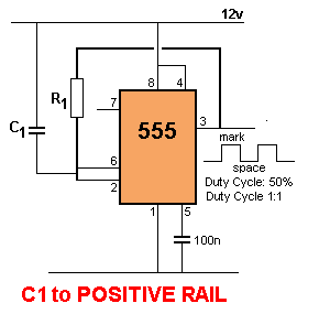


C1 to 0v rail
C1 to 12v rail
1k1n505kHz1k1n255kHz
1k10n115kHz1k10n130kHz
1k100n23kHz1k100n16kHz
10k1n112kHz10k1n128kHz
10k10n27kHz10k10n16kHz
10k100n3700Hz10k100n1600Hz

 
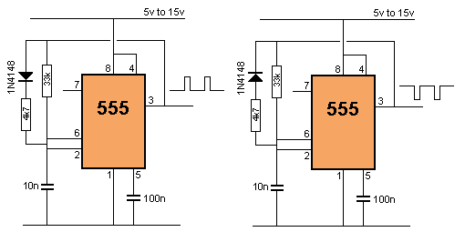
CHANGING THE MARK-SPACE RATIOThis ratio can be altered by adding a diode and resistor as shown in the following diagrams. In the first diagram, the 555 comes ON ("fires-up") with pin 3 low and pin 2 immediately detects this low and makes pin 3 HIGH. The 10n is quickly charged via the diode and 4k7 and this is why the MARK is "short." When the capacitor is 2/3Vcc, pin 6 detects a HIGH and the output of the 555 goes LOW. The 10n is discharged via the 33k and this creates the long-duration SPACE (LOW). The second diagram creates a long-duration HIGH:

--------------------------------------------------------------------------------------------------------


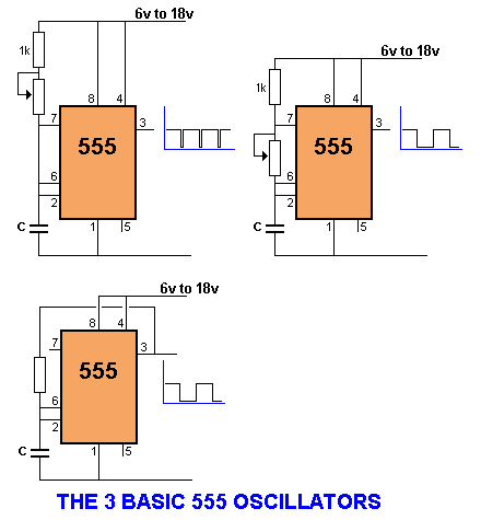
THE THREE BASIC 555 OSCILLATORSThe 3 basic 555 oscillators are shown in these circuits.
The basic points to remember are these:
Pin 7 goes LOW when pin 3 goes LOW.
Pin 6 detects a HIGH
Pin 2 detects a LOW
Pin 3 can be used instead of the supply-rail to deliver a HIGH and instead of pin 7 to deliver a LOW to the timing section made up of pins 2&6 and "C" and a timing resistor.


----------------------------------------------------------------------------------------------------------------------------------


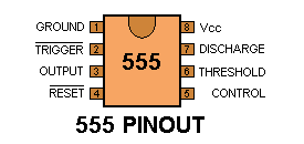
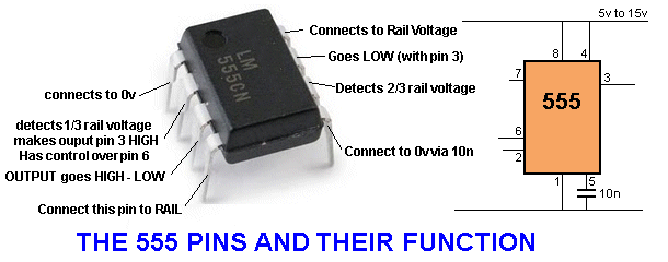
HOW TO REMEMBER THE PINS:
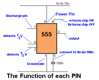
---------------------------------------------------------------------------------

INSIDE THE 555 

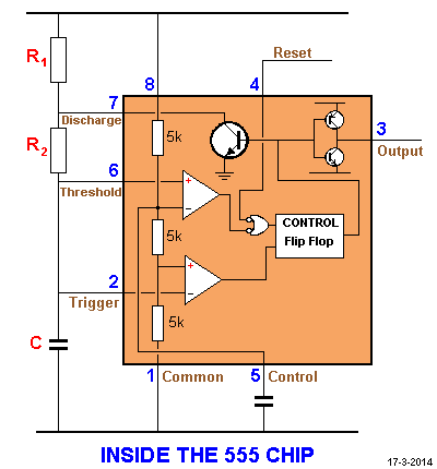
Note: Pin 7 is "in phase" with output Pin 3 (both are low at the same time).
Pin 7 "shorts" to 0v via a transistor. It is pulled HIGH via R1.
Maximum supply voltage 16v - 18v
Current consumption approx 10mA
Output Current sink @5v = 5 - 50mA     @15v = 50mA
Output Current source @5v = 100mA     @15v = 200mA
Maximum operating frequency 300kHz - 500kHz

Faults with Chip:
Consumes about 10mA when sitting in circuit
Output voltage can be up to 2.5v less than rail voltage Output can be  0.5v to 1.5v above groundSources up to 200mA
Some chips sink only 50mA,  some will sink 200mA

A NE555 was tested at 1kHz, 12.75v rail and 39R load. 
The Results: 
Output voltage 0.5v low, 11.5v high at output current of 180mA 
The "test chip" performance was excellent.

-------------------------------------------------------------------------------------------------------------------------------------------------------------------


THE 555 PINS

No comments:
Here is the identification for each pin:

When drawing a circuit diagram, always draw the 555 as a building block, as shown below with the pins in the following locations. This will help you instantly recognise the function of each pin:


Pin 1 GROUND.  Connects to the 0v rail. Pin 2 TRIGGER. Detects 1/3 of rail voltage to make output HIGH. Pin 2 has control over pin 6. If pin 2 is LOW, and pin 6 LOW,  output goes and stays HIGH. If pin 6 HIGH, and pin 2 goes LOW, output goes LOW while pin 2 LOW. This pin has a very high impedance (about 10M) and will trigger with about 1uA.Pin 3 OUTPUT. (Pins 3 and 7 are "in phase.") Goes HIGH (about 2v less than rail) and LOW (about 0.5v above 0v rail) and will deliver up to 200mA.Pin 4 RESET. Internally connected HIGH via 100k. Must be taken below 0.8v to reset the chip. Pin 5 CONTROL. A voltage applied to this pin will vary the timing of the RC network (quite considerably).  Pin 6 THRESHOLD.  Detects 2/3 of rail voltage to make output LOW only if pin 2 is HIGH. This pin has a very high impedance (about 10M) and will trigger with about 1uA.Pin 7 DISCHARGE. Goes LOW when pin 6 detects 2/3 rail voltage but pin 2 must be HIGH. If pin 2 is HIGH, pin 6 can be HIGH or LOW and pin 7 remains LOW. Goes OPEN (HIGH) and stays HIGH when pin 2 detects 1/3 rail voltage (even as a LOW pulse) when pin 6 is LOW.  (Pins 7 and 3 are "in phase.") Pin 7 is equal to pin 3 but pin 7 does not go high - it goes OPEN.  But it goes LOW and will sink about 200mA. You can connect pin 7 to pin 3 to get a slightly better SINK capability from the chip.Pin 8 SUPPLY. Connects to the positive rail.


555 LED DIMMER Circuit

No comments:
This circuit will adjust the brightness of one or more LEDs from 5% to 95%.


Electronics lab created by Muhammad Irfan 
Electronics lab created by Muhammad Irfan

555 Amplifier Circuit

No comments:
The 555 can be used as an amplifier. It operates very similar to pulse-width modulation. The component values cause the 555 to oscillate at approx 66kHz and the speaker does not respond to this high frequency.  Instead it responds to the average CD value of the modulated output and demonstrates the concept of pulse-width modulation. The chip gets very hot and is only for brief demonstrations. 


Electronics Lab  created   By   Muhammad Irfan