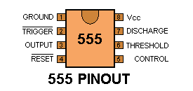
Here is the identification for each pin:
When drawing a circuit diagram, always draw the 555 as a building block, as shown below with the pins in the following locations. This will help you instantly recognise the function of each pin:
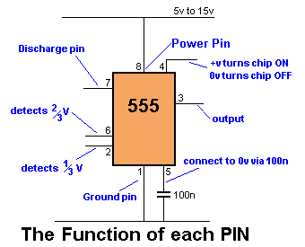
Pin 1 GROUND. Connects to the 0v rail. Pin 2 TRIGGER. Detects 1/3 of rail voltage to make output HIGH. Pin 2 has control over pin 6. If pin 2 is LOW, and pin 6 LOW, output goes and stays HIGH. If pin 6 HIGH, and pin 2 goes LOW, output goes LOW while pin 2 LOW. This pin has a very high impedance (about 10M) and will trigger with about 1uA.Pin 3 OUTPUT. (Pins 3 and 7 are "in phase.") Goes HIGH (about 2v less than rail) and LOW (about 0.5v above 0v rail) and will deliver up to 200mA.Pin 4 RESET. Internally connected HIGH via 100k. Must be taken below 0.8v to reset the chip. Pin 5 CONTROL. A voltage applied to this pin will vary the timing of the RC network (quite considerably). Pin 6 THRESHOLD. Detects 2/3 of rail voltage to make output LOW only if pin 2 is HIGH. This pin has a very high impedance (about 10M) and will trigger with about 1uA.Pin 7 DISCHARGE. Goes LOW when pin 6 detects 2/3 rail voltage but pin 2 must be HIGH. If pin 2 is HIGH, pin 6 can be HIGH or LOW and pin 7 remains LOW. Goes OPEN (HIGH) and stays HIGH when pin 2 detects 1/3 rail voltage (even as a LOW pulse) when pin 6 is LOW. (Pins 7 and 3 are "in phase.") Pin 7 is equal to pin 3 but pin 7 does not go high - it goes OPEN. But it goes LOW and will sink about 200mA. You can connect pin 7 to pin 3 to get a slightly better SINK capability from the chip.Pin 8 SUPPLY. Connects to the positive rail.
When drawing a circuit diagram, always draw the 555 as a building block, as shown below with the pins in the following locations. This will help you instantly recognise the function of each pin:
Pin 1 GROUND. Connects to the 0v rail. Pin 2 TRIGGER. Detects 1/3 of rail voltage to make output HIGH. Pin 2 has control over pin 6. If pin 2 is LOW, and pin 6 LOW, output goes and stays HIGH. If pin 6 HIGH, and pin 2 goes LOW, output goes LOW while pin 2 LOW. This pin has a very high impedance (about 10M) and will trigger with about 1uA.Pin 3 OUTPUT. (Pins 3 and 7 are "in phase.") Goes HIGH (about 2v less than rail) and LOW (about 0.5v above 0v rail) and will deliver up to 200mA.Pin 4 RESET. Internally connected HIGH via 100k. Must be taken below 0.8v to reset the chip. Pin 5 CONTROL. A voltage applied to this pin will vary the timing of the RC network (quite considerably). Pin 6 THRESHOLD. Detects 2/3 of rail voltage to make output LOW only if pin 2 is HIGH. This pin has a very high impedance (about 10M) and will trigger with about 1uA.Pin 7 DISCHARGE. Goes LOW when pin 6 detects 2/3 rail voltage but pin 2 must be HIGH. If pin 2 is HIGH, pin 6 can be HIGH or LOW and pin 7 remains LOW. Goes OPEN (HIGH) and stays HIGH when pin 2 detects 1/3 rail voltage (even as a LOW pulse) when pin 6 is LOW. (Pins 7 and 3 are "in phase.") Pin 7 is equal to pin 3 but pin 7 does not go high - it goes OPEN. But it goes LOW and will sink about 200mA. You can connect pin 7 to pin 3 to get a slightly better SINK capability from the chip.Pin 8 SUPPLY. Connects to the positive rail.
Electronics Lab Created by Muhammad Irfan
Electronics Lab Created by Muhammad Irfan


No comments:
Post a Comment