Saturday, November 16, 2013

Water level controller using 8051

No comments:
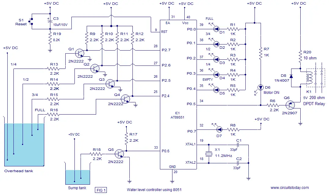
 A water level controller based using 8051 is shown in this article. A lot of water level controller projects have been published in this website but the is the first one based on a microcontroller. This water level controller monitors the level of the over head tank  and automatically switches on the water pump when ever the level goes below a preset limit. The level of the over head tank is indicated using 5 leds and the pump is switched of when the over head tank is filled. The pump is not allowed to start if the water level in the sump tank is low and also the pump is switched off when the level inside the sump tank goes low during a pumping cycle. The circuit diagram of the water level controller is shown below.

The level sensor probes for the overhead tank are interfaced to the port 2 of the microcontroller through transistors. Have a look at the sensor probe arrangement for the overhead tank in Fig1. A positive voltage supply probe goes to the down bottom of the tank. The probes for sensing 1/4, 1/2, 3/4 and FULL levels are placed with equal spacing one by one above the bottom positive probe. Consider the topmost (full level) probe, its other end is connected to the base of transistor Q4 through resistor R16. Whenever water rises to the full level current flows into the base of transistor Q4 which makes it ON and so its collector voltage goes low. The collector of Q4 is connected to P2.4 and a low voltage at  P2.4 means the over head tank is not FULL. When water level goes below the full level probe, the base of Q2 becomes open making it OFF. Now its collector voltage goes high and high at P2.4 means the tank is not full. The same applies to other sensor probes (3/4, 1/2, 1/4) and the microprocessor understands the current level by scanning the port pins P2.4 ,P2.5, P2.6 and P2.7. All these port pin are high (all sensor probes are open) means the tank is empty.
Port pin P0.5 is used to control the pump. When ever it is required start pumping, the controller makes P0.5 low which makes transistor Q6 ON which in turn activates the relay K1 that switches the pump. Also the LED d6 glows indicating the motor is ON. LED D7 is the low sump indicator. When the water level in the sump tank goes low, the controller makes P0.7 low which makes LED D7 to glow. The circuit diagram of the water level controller is shown in the figure below.

Circuit diagram.

water level controller using 8051
Water level controller using 8051

Program.

MOV P2,#11111111B // initiates P2 as sensor input
MOV P0,#11111111B // initiates P2 as the output port
MOV A,#00000000B
MAIN:ACALL SMPCK // checks the level of the sump tank
MOV A,P2 // moves the current status of P2 tp A
CJNE A,#11110000B,LABEL1 // checks whether tank is full
SETB P0.1
SETB P0.2
SETB P0.3
SETB P0.4
CLR P0.0 // glows full level LED
SETB P0.5
LABEL1:MOV A,P2
CJNE A,#11111000B,LABEL2 // checks whether tank is 3/4
SETB P0.0
SETB P0.2
SETB P0.3
SETB P0.4
CLR P0.1 // glows 3/4 level LED
LABEL2:MOV A,P2
CJNE A,#11111100B,LABEL3 // checks whether tank is 1/2
SETB P0.0
SETB P0.1
SETB P0.3
SETB P0.4
CLR P0.2 // glows 1/2 level LED
LABEL3:MOV A,P2
CJNE A,#11111110B,LABEL4 // checks whether tank is 1/4
SETB P0.0
SETB P0.1
SETB P0.2
SETB P0.4
CLR P0.3 // glows 1/4 level LED
JB P0.6,LABEL4
CLR P0.5 // switches motor ON
LABEL4:MOV A,P2
CJNE A,#11111111B,MAIN // checks whether tank is empty
SETB P0.0
SETB P0.1
SETB P0.2
SETB P0.3
CLR P0.4 // glows EMPTY LED
JB P0.6,MAIN // checks whether sump is low
CLR P0.5 // switches motor ON
SJMP MAIN
SMPCK:JB P0.6,LABEL5 // checks whether sump is low
SETB P0.7 // extinguishes the sump low indicator LED
SJMP LABEL6
LABEL5:SETB P0.5 // switches the pump OFF
CLR P0.7 // glows sump low indicator LED
LABEL6:RET
END


http://www.mediafire.com/?f01f1242yfl2tf1

Digital tachometer using 8051

No comments:

Contact less digital tachometer using 8051.

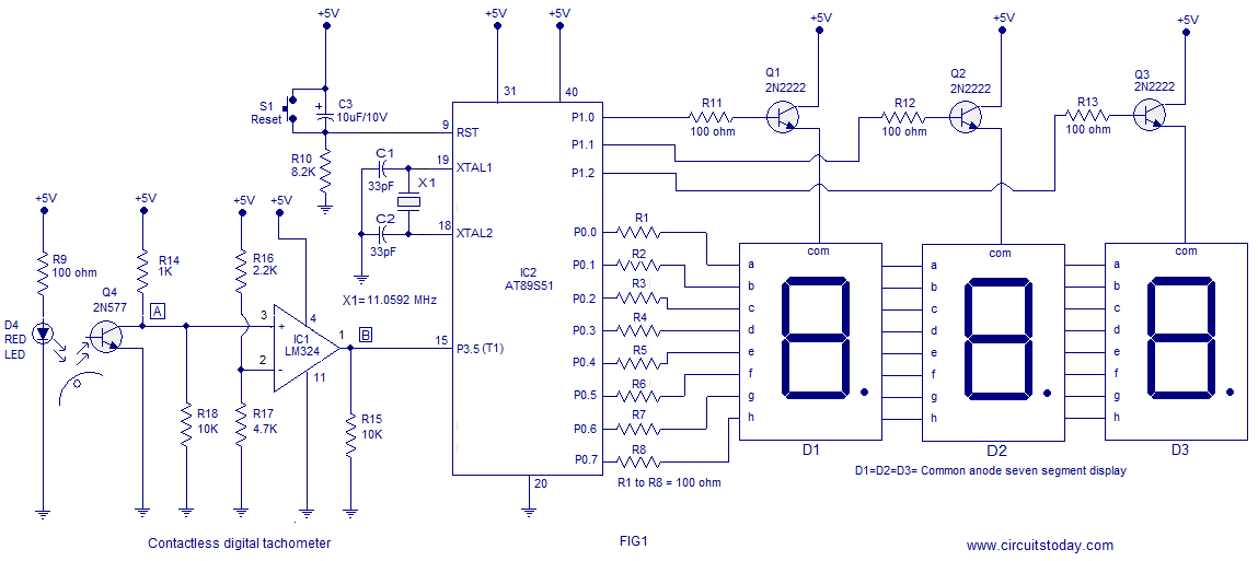
A three digit contact less digital tachometer using 8051 microcontroller which can be used for measuring the revolutions/second of a rotating wheel, disc, shaft or anything like that is introduced in this project. The tachometer  can measure up to a maximum of 255 rev/sec at an accuracy of 1 rev/sec. What you just need to do is to align the sensor close to the reflective strip  (aluminium foil, white paper or some thing like that) glued on the rotating surface and the meter shows the rev/sec on the display.
The circuit diagram of the digital tachometer is shown below.

Digital tachometer using 8051
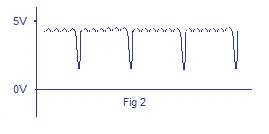
The first section of the circuit is the optical pickup based on photo transistor Q4 and red LED D4. Every time the reflective stripe  on the rotating object passes in front of  the sensor assembly, the reflected light falls on the photo transistor which makes it conduct more and as a result  its collector voltage drops towards zero. When viewed through an oscilloscope the collector waveform of the photo transistor Q4 (2N5777) would look like this:
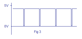
optical pick up outputNext part is the signal conditioning unit based on the opamp LM324 (IC1). Only one opamp inside the quad LM324 is used here and it is wired as a comparator with reference voltage set at 3.5V (using resistors  R16 and R17). The job of this comparator unit is to convert the spiky collector wave form into a neat square pulse train so that it can be applied to the microcontroller. Every time the collector voltage of the photo transistor goes below 3.5V, the output of the comparator goes to negative saturation and every time the collector voltage of the photo transistor goes above 3.5V, the comparator output goes to positive saturation resulting in a waveform like this:
         tachometer optical pickup output
From the above two graphs you can see that the negative going edge of the waveform indicates the passage of the reflective patch across the sensor and that means one revolution. If you could some how measure the number of negative going edges occurring in one second, then that’s the rev/sec of the rotating object and that’s what the microcontroller does here.
The 8051 microcontroller here does two jobs and they are:
1)  Count the number of negative going pulses available at its T1 pin (pin15).
2) Do necessary mathematics and display the count on the 3 digit 7 segment display.
For the counting purpose both the timers of 8051 (Timer0 and Timer1) are used. Timer 1 is configured as an 8 bit auto reload counter for registering the number of incoming zero going pulses and Timer0 is configured as a 16 bit timer which generate the necessary 1 second time span for the Timer1 to count.

Program.

ORG 000H
MOV DPTR,#LUT              // moves the addres of LUT to DPTR
MOV P1,#00000000B          // Sets P1 as an output port
MOV P0,#00000000B          // Sets P0 as an output port
MAIN: MOV R6,#14D
      SETB P3.5
      MOV TMOD,#01100001B  // Sets Timer1 as Mode2 counter & Timer0 as Mode1 timer
      MOV TL1,#00000000B   //loads initial value to TL1
      MOV TH1,#00000000B   //loads initial value to TL1
      SETB TR1             // starts timer(counter) 1
BACK: MOV TH0,#00000000B   //loads initial value to TH0
      MOV TL0,#00000000B   //loads initial value to TH0
      SETB TR0             //starts timer 0
HERE: JNB TF0,HERE         // checks for Timer 0 roll over
      CLR TR0              // stops Timer0
      CLR TF0              // clears Timer Flag 0
      DJNZ R6,BACK
      CLR TR1              // stops Timer(counter)1
      CLR TF0              // clears Timer Flag 0
      CLR TF1              // clears Timer Flag 1
      ACALL DLOOP          // Calls subroutine DLOOP for displaying the count
      SJMP MAIN            // jumps back to the main loop
DLOOP: MOV R5,#100D
BACK1: MOV A,TL1           // loads the current count to the accumulator
       MOV B,#100D
       DIV AB              // isolates the first digit of the count
       SETB P1.0
       ACALL DISPLAY       // converts the 1st digit to 7 seg pattern
       MOV P0,A            // puts the pattern to Port 0
       ACALL DELAY         // 1mS delay
       ACALL DELAY
       MOV A,B
       MOV B,#10D
       DIV AB              // isolates the secong digit of the count
       CLR P1.0
       SETB P1.1
       ACALL DISPLAY       // converts the 2nd digit to 7 seg pattern
       MOV P0,A
       ACALL DELAY
       ACALL DELAY
       MOV A,B             // moves the last digit of the count to accumulator
       CLR P1.1
       SETB P1.2
       ACALL DISPLAY       // converts the 3rd digit to 7 seg pattern
       MOV P0,A
       ACALL DELAY
       ACALL DELAY
       CLR P1.2
       DJNZ R5,BACK1       // repeats the subroutine DLOOP 100 times
       RET

DELAY: MOV R7,#250D        // 1mS delay
 DEL1: DJNZ R7,DEL1
       RET

DISPLAY: MOVC A,@A+DPTR    // gets 7 seg digit drive pattern for current value in A
         CPL A             //  (See Note 1)
         RET
LUT: DB 3FH                // Look up table (LUT) starts here
     DB 06H
     DB 5BH
     DB 4FH
     DB 66H
     DB 6DH
     DB 7DH
     DB 07H
     DB 7FH
     DB 6FH
END

Notes.

1) The LUT used here was made for a common cathode seven segment display (used in previous projects) and here we are using a common anode display. The instruction CPL A will just complement the digit drive pattern in accumulator so that it becomes suitable for the common anode display. This is done just because to save my time but not a text book method. The correct way is to make a dedicated LUT for common anode configuration and aviod the extra CPL A instruction.
2) LM324 is a quad opamp and only one opamp inside it is used here. I used LM324 just because that was the only single supply opamp with me at the time. You can use any single supply opamp that matches our supply voltage(5V). You can even use a dual supply opamp (like the popular 741) in single supply mode (+V pin connected to positive supply and -V pin connected to ground) but i wont recommend it unless you have an oscilloscope. Dual supply opamps configured in single supply mode will not give results like a dedicated single supply opamp in the same situation.
3) As we saw earlier the Timer 0 which generates the 1 second time span is configured in Mode 1 (16 bit timer). So the maximum it can count is 2^16 and that is 65536. In 8051 the crystal frequency is divided by 12 using an internal network before applying it as a clock for the timer. That means the timer will increment by one for every 1/12th of the crystal frequency. For an 8051 system clocked with a 12MHz crystal the time taken for one timer increment will be 1µS (ie; 1/12MHz). So the maximum time delay that can be obtained using one session of the timer will be 65536µS and it is looped 14 times to get the 1 second delay. Go through this article Delay using 8051 timer for a better grasp.

Digital thermometer using 8051

No comments:
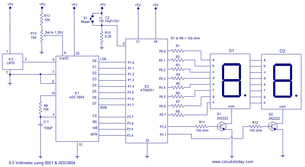
This article is about a simple 0-100°C digital thermometer with 1°C resolution using 8051. The circuit is based on LM35 analog temperature sensor, ADC0804 and AT89S51 microcontroller. LM35 is an analogue temperature sensor IC which can measure a temperature range of -55 to 150°C. Its output voltage varies 10mV per °C change in temperature.
For example, if the temperature is 32°C, the output voltage will be 32 x 10mV = 320mV. ADC 0804 is used to convert the analogue output voltage of the LM35  to a proportional 8 bit digital value suitable for the microcontroller. The microcontroller accepts the output of ADC, performs necessary manipulations on it and displays it numerically on a 2 digit seven segment LED display.
Out put of the LM35 is connected to the +Vin (pin 6) of the ADC0804. Resistor R13 and preset R14 is used to provide an external reference voltage of 1.28V to the Vref/2 pin  ( pin 9) of the ADC0804 and with this reference voltage, the step size of the ADC will be 10mV and span will be 0-1 V. This means that for a 10mV input the digital out of ADC will be 1 (1 in decimal also), for 20mV it will be 10 (2 in decimal), for 30mV it will be 11 (3 in decimal) and so on. The microcontroller accepts this data and puts it on the seven segment display. 

Circuit diagram.

8051 digital thermometer
Digital thermometer using 8051
Digital out of the ADC (D0 to D7) are connected to P1 (P1.0 to P1.7) of the microcontroller. This is the line through which the microcontroller accepts data from the ADC. The control pins CS, RD, WR and  INTR are connected to P3.7, P3.6, P3.5 and P3.4 of the microcontroller. This is the data path through which the microcontroller sends chip select (CS), read (RD) write (WR) signals to the ADC and receives INTR signal from the ADC. Data lines (a to h) of the multiplexed seven segment display are interfaced to P0 (P0.0 to P0.7) of the microcontroller. Activation signals for the segment driver transistors Q1 and Q2 are available from P3.2 and P3.1 pins of the microcontroller. 
Before attempting this circuit go through these articles Voltmeter using 8051  , Interfacing ADC to 8051 ,Interfacing seven segment display to 8051

Program.

ORG 00H
MOV P1,#11111111B   // initializes P1 as input port
MOV P0,#00000000B   // initializes P0 as output port
MOV P3,#00000000B   // initializes P3 as output port
MOV DPTR,#LABEL     // loads the address of "LABEL" to DPTR
MAIN: MOV R4,#250D  // loads register R4 with 250D
      CLR P3.7      // makes Cs=0
      SETB P3.6     // makes RD high
      CLR P3.5      // makes WR low
      SETB P3.5     // low to high pulse to WR for starting conversion
WAIT: JB P3.4,WAIT  // polls until INTR=0
      CLR P3.7      // ensures CS=0
      CLR P3.6      // high to low pulse to RD for reading the data from ADC
      MOV A,P1      // moves the digital output of ADC to accumulator A
      MOV B,#10D    // load B with 10D
      DIV AB        // divides the content of A with that in B
      MOV R6,A      // moves the quotient to R6
      MOV R7,B      // moves the remainder to R7
DLOOP:SETB P3.2     // sets P3.2 which activates LED segment 1
      MOV A,R6      // moves the quotient to A
      ACALL DISPLAY // calls DISPLAY subroutine
      MOV P0,A      // moves the content of A to P0
      ACALL DELAY   // calls the DELAY subroutine
      CLR A         // clears A
      MOV A,R7      // moves the remainder to A
      CLR P3.2      // deactivates LED segment 1
      SETB P3.1     // activates LED segment 2
      ACALL DISPLAY
      MOV P0,A
      ACALL DELAY
      CLR A
      CLR P3.1      // deactivates LED segment 2
      DJNZ R4,DLOOP // repeats the loop "DLOOP" until R4=0
      SJMP MAIN     // jumps back to the main loop
DELAY: MOV R3,#255D // produces around 0.8mS delay
LABEL1: DJNZ R3,LABEL1
        RET
DISPLAY: MOVC A,@A+DPTR // converts A's content to corresponding digit drive pattern
         RET
LABEL: DB 3FH       // LUT (look up table) starts here
       DB 06H
       DB 5BH
       DB 4FH
       DB 66H
       DB 6DH
       DB 7DH
       DB 07H
       DB 7FH
       DB 6FH
END