8051 Microcontroller/8051 Microcontroller Architecture
A micro controller is
an integrated circuit or a chip with a processor and other support
devices like program memory, data memory, I/O ports, serial
communication interface etc integrated together. Unlike a microprocessor
(ex: Intel 8085), a microcontroller does not require
any external interfacing of support devices. Intel 8051 is the most
popular microcontroller ever produced in the world market. Now lets talk
about 8051 microcontroller in detail.
Before going further, it will be interesting for you to understand the difference between a Microprocessor and Microcontroller. We have a detailed article which describes the basic difference between both.
Here is a Quick Access to various sections of this article:-
Introduction
Intel first produced a microcontroller in 1976 under the name MCS-48, which was an 8 bit
microcontroller. Later in 1980 they released a further improved version
(which is also 8 bit), under the name MCS-51. The most popular
microcontroller 8051 belongs to the MCS-51 family of microcontrollers by
Intel. Following the success of 8051, many other semiconductor
manufacturers released microcontrollers under their own brand name but
using the MCS-51 core. Global companies and giants in semiconductor
industry like Microchip, Zilog, Atmel, Philips, Siemens
released products under their brand name. The specialty was that all
these devices could be programmed using the same MCS-51 instruction
sets. They basically differed in support device configurations like
improved memory, presence of an ADC or DAC etc. Intel then released its
first 16 bit microcontroller in 1982, under name MCS-96
8051 Microcontroller Packaging
There is no need of explaining what each
package means, you already know it. So I will skim through mainly used
packaging for 8051. See, availability of various packages change from
device to device. The most commonly used is Dual Inline Package (40
pins) – known popularly as DIP. 8051 is also available in QFP (Quad Flat
Package), TQFP (Thin Quad Flat Package), PQFP (Plastic Quad Flat
Package) etc. For explaining the pin diagram, we have used a 40 pin DIP
IC as model.
8051 Microcontroller Architecture
Its possible to explain microcontroller
architecture to a great detail, but we are limiting scope of this
article to internal architecture, pin configuration, program memory and
data memory organization. The basic architecture remains same for the
MCS-51 family. In general all microcontrollers in MCS- 51 family are
represented by XX51, where XX can take values like 80, 89 etc.
Schematic and Features

8051 Microcontroller
A micro controller
is an integrated circuit or a chip with a processor and other support
devices like program memory, data memory, I/O ports, serial
communication interface etc integrated together. Unlike a microprocessor
(ex: Intel 8085), a microcontroller does not require
any external interfacing of support devices. Intel 8051 is the most
popular microcontroller ever produced in the world market. Now lets talk
about 8051 microcontroller in detail.
Before going further, it will be interesting for you to understand the difference between a Microprocessor and Microcontroller. We have a detailed article which describes the basic difference between both.
Microprocessor vs Microcontroller
Here is a Quick Access to various sections of this article:-
Pin Diagram :- Internal Architecture :- Program Memory Organization :- Data Memory Organization :-8051 System Clock :- 8051 Reset Circuit
Introduction
Intel first produced a microcontroller in 1976 under the name MCS-48, which was an 8 bit
microcontroller. Later in 1980 they released a further improved version
(which is also 8 bit), under the name MCS-51. The most popular
microcontroller 8051 belongs to the MCS-51 family of microcontrollers by
Intel. Following the success of 8051, many other semiconductor
manufacturers released microcontrollers under their own brand name but
using the MCS-51 core. Global companies and giants in semiconductor
industry like Microchip, Zilog, Atmel, Philips, Siemens
released products under their brand name. The specialty was that all
these devices could be programmed using the same MCS-51 instruction
sets. They basically differed in support device configurations like
improved memory, presence of an ADC or DAC etc. Intel then released its
first 16 bit microcontroller in 1982, under name MCS-96
8051 Microcontroller Packaging
There is no need of explaining what each
package means, you already know it. So I will skim through mainly used
packaging for 8051. See, availability of various packages change from
device to device. The most commonly used is Dual Inline Package (40
pins) – known popularly as DIP. 8051 is also available in QFP (Quad Flat
Package), TQFP (Thin Quad Flat Package), PQFP (Plastic Quad Flat
Package) etc. For explaining the pin diagram, we have used a 40 pin DIP
IC as model.
8051 Microcontroller Architecture
Its possible to explain microcontroller
architecture to a great detail, but we are limiting scope of this
article to internal architecture, pin configuration, program memory and
data memory organization. The basic architecture remains same for the
MCS-51 family. In general all microcontrollers in MCS- 51 family are
represented by XX51, where XX can take values like 80, 89 etc.
Schematic and Features

The general schematic diagram of 8051
microcontroller is shown above. We can see 3 system inputs, 3 control
signals and 4 ports (for external interfacing). A Vcc power supply and
ground is also shown. Now lets explain and go through each in detail.
System inputs are necessary to make the micro controller functional. So
the first and most important of this is power, marked as Vcc with a GND
(ground potential). Without proper power supply, no electronic system
would work. XTAL 1 and XTAL 2 are for the system clock inputs from
crystal clock circuit. RESET input is required to initialize
microcontroller to default/desired values and to make a new start.
There are 3 control signals, EA,PSEN and
ALE. These signals known as External Access (EA), Program Store Enable
(PSEN), and Address Latch Enable (ALE) are used for external memory
interfacing.
Take a look at the schematic diagram below (a functional microcontroller)

As mentioned above, control signals are
used for external memory interfacing. If there is no requirement of
external memory interfacing then, EA pin is pulled high (connected to
Vcc) and two others PSEN and ALE are left alone. You can also see a 0.1
micro farad decoupling capacitor connected to Vcc (to avoid HF
oscillations at input).
There are four ports numbered 0,1,2,3
and called as Port 0, Port 1, Port 2 and Port 3 which are used for
external interfacing of devices like DAC, ADC, 7 segment display, LED
etc. Each port has 8 I/O lines and they all are bit programmable.
8051 Pin Diagram & Description

For describing pin diagram and pin
configuration of 8051, we are taking into consideration a 40 pin DIP
(Dual inline package). Now lets go through pin configuration in detail.
Pin-40 : Named as Vcc is the main power source. Usually its +5V DC.
You may note some pins are designated with two signals (shown in brackets).
Pins 32-39: Known as
Port 0 (P0.0 to P0.7) – In addition to serving as I/O port, lower order
address and data bus signals are multiplexed with this port (to serve
the purpose of external memory interfacing). This is a bi directional
I/O port (the only one in 8051) and external pull up resistors are
required to function this port as I/O.
Pin-31:- ALE aka
Address Latch Enable is used to demultiplex the address-data signal of
port 0 (for external memory interfacing.) 2 ALE pulses are available
for each machine cycle.
Pin-30:- EA/ External
Access input is used to enable or disallow external memory interfacing.
If there is no external memory requirement, this pin is pulled high by
connecting it to Vcc.
Pin- 29:- PSEN or Program Store Enable is used to read signal from external program memory.
Pins- 21-28:- Known as
Port 2 (P 2.0 to P 2.7) – in addition to serving as I/O port, higher
order address bus signals are multiplexed with this quasi bi directional
port.
Pin 20:- Named as Vss – it represents ground (0 V) connection.
Pins 18 and 19:- Used for interfacing an external crystal to provide system clock.
Pins 10 – 17:- Known as
Port 3. This port also serves some other functions like interrupts,
timer input, control signals for external memory interfacing RD and WR ,
serial communication signals RxD and TxD etc. This is a quasi bi
directional port with internal pull up.
Pin 9:- As explained
before RESET pin is used to set the 8051 microcontroller to its initial
values, while the microcontroller is working or at the initial start of
application. The RESET pin must be set high for 2 machine cycles.
Pins 1 – 8:- Known as
Port 1. Unlike other ports, this port does not serve any other
functions. Port 1 is an internally pulled up, quasi bi directional I/O
port.
8051 Internal Architecture
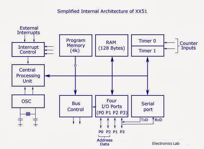
There is no need of any detailed
explanation to understand internal architecture of 8051 micro
controller. Just look at the diagram above and you observer it
carefully. The system bus connects all the support devices with the
central processing unit. 8051 system bus composes of an 8 bit data bus
and a 16 bit address bus and bus control signals. From the figure you
can understand that all other devices like program memory, ports, data
memory, serial interface, interrupt control, timers, and the central
processing unit are all interfaced together through the system bus. RxD
and TxD (serial port input and output) are interfaced with port 3.
8051 Memory Organization
Before going deep into the memory
architecture of 8051, lets talk a little bit about two variations
available for the same. They are Princeton architecture and Harvard
architecture. Princeton architecture treats address memory and data
memory as a single unit (does not distinguish between two) where as
Harvard architecture treats program memory and data memory
as separate entities. Thus Harvard architecture demands address, data
and control bus for accessing them separately where as Princeton
architecture does not demand any such separate bus.
Example:- 8051 micro controller is based on Harvard architecture and 8085 micro processor is based on Princeton architecture.
Thus 8051 has two memories :- Program memory and Data memory
Program memory organization

Now lets dive into the program memory
organization 0f 8051. It has an internal program of 4K size and if
needed an external memory can be added (by interfacing ) of size 60K
maximum. So in total 64K size memory is available for 8051 micro
controller. By default, the External Access (EA) pin should be
connected Vcc so that instructions are fetched from internal memory
initially. When the limit of internal memory (4K) is crossed, control
will automatically move to external memory to fetch remaining
instructions. If the programmer wants to fetch instruction from external
memory only (bypassing the internal memory), then he must connect
External Access (EA) pin to ground (GND).
You may already know that 8051 has a
special feature of locking the program memory (internal) and hence
protecting against software piracy. This feature is enable by program
lock bits. Once these bits are programmed, contents of internal memory
can not be accessed using an external circuitry. How ever locking the
software is not possible if external memory is also used to store the
software code. Only internal memory can be locked and protected. Once
locked, these bits can be unlocked only by a memory-erase operation,
which in turn will erase the programs in internal memory too.
8051 is capable of pipelining.
Pipelining makes a processor capable of fetching the next instruction
while executing previous instruction. Its some thing like multi tasking,
doing more than one operation at a time. 8051 is capable of fetching
first byte of the next instruction while executing the previous
instruction.
Data memory organization

In the MCS-51 family, 8051 has 128 bytes of internal data memory and it
allows interfacing external data memory of maximum size up to 64K. So
the total size of data memory in 8051 can be upto 64K (external) + 128
bytes (internal). Observe the diagram carefully to get more
understanding. So there are 3 separations/divisions of the data memory:-
1) Register banks 2) Bit addressable area 3) Scratch pad area.

Register banks form the lowest 32 bytes
on internal memory and there are 4 register banks designated bank #0,#1,
#2 and #3. Each bank has 8 registers which are designated as R0,R1…R7.
At a time only one register bank is selected for operations and the
registers inside the selected bank are accessed using mnemonics R0..R1..
etc. Other registers can be accessed simultaneously only by direct
addressing. Registers are used to store data or operands during
executions. By default register bank #0 is selected (after a system
reset).
The bit addressable ares of 8051 is
usually used to store bit variables. The bit addressable area is formed
by the 16 bytes next to register banks. They are designated from address
20H to 2FH (total 128 bits). Each bits can be accessed from 00H to 7FH
within this 128 bits from 20H to 2FH. Bit addressable area is mainly
used to store bit variables from application program, like status of an
output device like LED or Motor (ON/OFF) etc. We need only a bit to
store this status and using a complete byte addressable area for storing
this is really bad programming practice, since it results in wastage of
memory.
The scratch pad area is the upper 80
bytes which is used for general purpose storage. Scratch pad area is
from 30H to 7FH and this includes stack too.
8051 System Clock

An 8051 clock circuit is shown above.
In general cases, a quartz crystal is used to make the clock circuit.
The connection is shown in figure (a) and note the connections to XTAL 1
and XTAL 2. In some cases external clock sources are used and you can
see the various connections above. Clock frequency limits (maximum and
minimum) may change from device to device. Standard practice is to use
12MHz frequency. If serial communications are involved then its best to
use 11.0592 MHz frequency.

Okay, take a look at the above machine
cycle waveform. One complete oscillation of the clock source is called a
pulse. Two pulses forms a state and six states forms one machine cycle.
Also note that, two pulses of ALE are available for 1 machine cycle.
8051 Reset Circuit

8051 can be reset in two ways 1) is power-on reset – which resets the
8051 when power is turned ON and 2) manual reset – in which a reset
happens only when a push button is pressed manually. Two different
reset circuits are shown above. A reset doesn’t affect contents of
internal RAM. For reset to happen, the reset input pin (pin 9) must be
active high for atleast 2 machine cycles. During a reset operation :-
Program counter is cleared and it starts from 00H, register bank #0 is
selected as default, Stack pointer is initialized to 07H, all ports are
written with FFH.
Electronics Lab Created By Muhammad Irfan


No comments:
Post a Comment