Interfacing dot matrix LED display to 8051 microcontroller.
LED dot matrix display.
An LED dot matrix display consists of a matrix of LED’s arranged in a rectangular configuration. The desired character or graphics can be displayed by switching ON /OFF a desired configuration of LED’s. Common display configurations available are 7×5, 8×8, 7×15, etc. LED dot matrix can be used in simple display applications where the resolution is not a big concern. The figure below shows the arrangement of LEDs in a typical 7×5 dot matrix display.
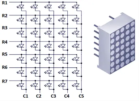
7x5 Led dot matrix display
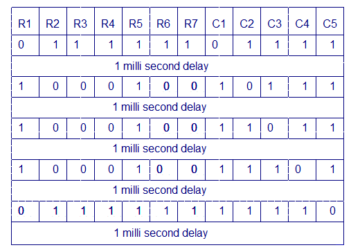
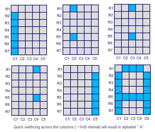
Any individual LED or a group of LEDs in the matrix can be activated by switching the required number of rows and columns. For example, in the above figure if Row1 is made high and Column1 is made low, the top left LED (address R1C1) will glow. As a demonstration, lets see how we can display letter “A” using the display. The tables given below shows the logic levels at each pin for displaying A.
In the above diagram you can see that only one LED in a row will be ON at a time but any number of LEDs in a column can be ON at a time. That means the microcontroller’s port pin can directly drive a row but it requires additional circuit for driving the column lines. The circuit diagram for interfacing dot matrix display and 8051 microcontroller is shown below.
Circuit diagram.
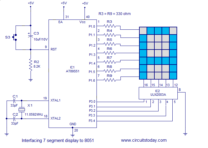
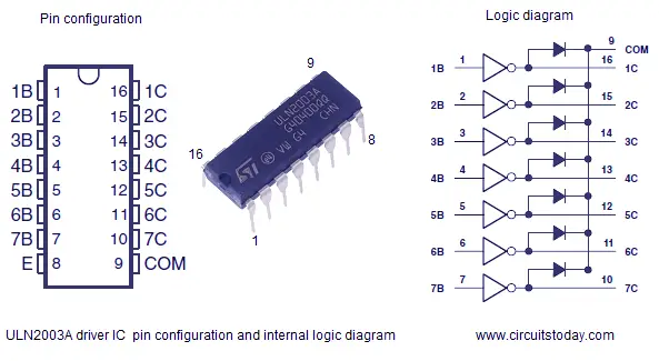
ULN2003A driver IC.
The purpose of ULN2003A here is to drive the column lines of the display. ULN2003A is a high voltage (50V), high current (500mA per channel) darlington transistor array. Each IC has 7 channels with individual output clamp diodes. ULN2003A an active high device, which means a logic high must be applied to the input to make the corresponding output high. The input pins are designated as 1B, 2B, 3B, 4B, 5B, 6B, 7B while corresponding output pins are designated as 1C, 2C, 3C, 4C, 5C, 6C, 7C. The pin configuration and simplified internal logic of ULN2003A is shown in the figure below.
Program.
ORG 00H
MOV P3,#00000000B        // initializes port 3 as output port
MOV P1,#00000000B        // initializes port 1 as output port
MAIN: MOV P3,#01111110B
      MOV P1,#11111110B
      ACALL DELAY
      MOV P3,#00010001B
      MOV P1,#11111101B
      ACALL DELAY
      MOV P3,#00010001B
      MOV P1,#11111011B
      ACALL DELAY
      MOV P3,#00010001B
      MOV P1,#11110111B
      ACALL DELAY
      MOV P3,#01111110B
      MOV P1,#11101111B
      ACALL DELAY
      SJMP MAIN         // jumps back to the main loop
DELAY: MOV R6,#255D     // 1ms delay subroutine
HERE: DJNZ R6,HERE
      RET
END
--------------------------------------------------------------------------------------------------------------
Electronics Lab Created By Muhammad Irfan
Electronics Lab Created By Muhammad Irfan


No comments:
Post a Comment