This article is all about how to interface push button switches to an
8051 microcontroller. Push button switches are widely used in embedded
system projects and the knowledge about interfacing them to 8051 is
very essential in designing such projects. A typical push button switch
has two active terminals that are normally open and these two terminals
get internally shorted when the push button is depressed. Images of a
typical pushbutton switch is shown below.
Circuit diagram.
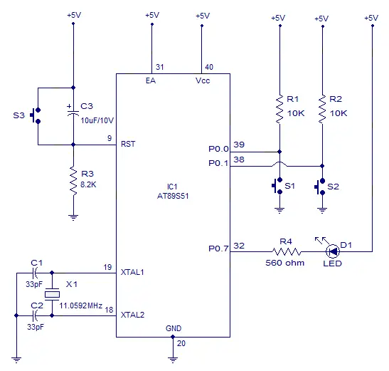
The circuit diagram for interfacing push button switch to 8051 is shown
above. AT89S51 is the microcontroller used here. The circuit is so
designed that when push button S1 is depressed the LED D1 goes ON and
remains ON until push button switch S2 is depressed and this cycle can
be repeated. Resistor R3, capacitor C3 and push button S3 forms the
reset circuitry for the microcontroller. Capacitor C1, C2 and crystal X1
belongs to the clock circuitry. R1 and R2 are pull up resistors for
the push buttons. R4 is the current limiting resistor for LED.
Program.
MOV P0,#83H // Initializing push button switches and initializing LED in OFF state.
READSW: MOV A,P0 // Moving the port value to Accumulator.
RRC A // Checking the vale of Port 0 to know if switch 1 is ON or not
JC NXT // If switch 1 is OFF then jump to NXT to check if switch 2 is ON
CLR P0.7 // Turn ON LED because Switch 1 is ON
SJMP READSW // Read switch status again.
NXT: RRC A // Checking the value of Port 0 to know if switch 2 is ON or not
JC READSW // Jumping to READSW to check status of switch 1 again (provided switch 2 is OFF)
SETB P0.7 // Turning OFF LED because Switch 2 is ON
SJMP READSW // Jumping to READSW to read status of switch 1 again.
END
The Logic
The first instruction – MOV P0 #83H -
is to turn LED off (Hex 83 in binary = 10000011) and to initialize
switches 1 and 2. Switch 1 is connected to port 0.0 and switch 2 is
connected to port 0.1. Also note that LED is connected to port 0.7.
Note:- Po.0
= 1 means switch 1 is OFF and Po.1 = 1 means switch 2 is OFF. P0.0 = o
means switch 1 is ON and p0.1 = o means switch 2 is ON. LED turns ON
when P0.7 = 0 and turns OFF when P0.7 = 1
The program has two labels – READSW and NXT. It’s all about reading
switch values – that is P0.0 and P0.1. We are using RRC instruction to
read switch values. The values of port 0 is moved to accumulator. Since
port 0 and 1 are used to interface switches 1 and 2, we can get the
values of both port bits in LSB”s 0 and 1 of accumulator by using MOV
A,P0 instruction. RRC – means – rotate right through carry. . What
RRC do is simple – it will move value of port 0.0 to the carry bit. Now
we can check the carry bit using instruction JC – which means “jump if
carry is set” . If carry is SET – then it means port0.0 =1 and this
means switch 1 is OFF. If switch 1 is OFF then we have to check status
of switch 2 and that is why we jump to label NXT.
In the mean time if switch 1 is pressed – then value of port 0.0 will be
equal to zero. This will get moved to accumulator and hence an RRC will
result in carry bit = o. If carry bit = 0 then result of executing JC
instruction is negative and it will not jump. The next instruction will
get executed – that is CLR P0.7. This clears port 0.7 to zero and hence
LED will turn ON. Once turned On- LED will be kept On until switch 2 is
pressed.
The status of switch 2 is checked in NXT label. When NXT is executed, we
are using RRC for the second time consecutively. This means, the carry
bit now holds the value of P0.1 – which is status of switch 2. If carry
bit = 1 then switch 2 is OFF. This means LED should not be turned OFF.
If carry bit = 0 then LED should be turned OFF (The instruction SETB
P0.7 turns LED OFF)
Toggling 2 LED with a pushbutton using interrupt.
This circuit demonstrates how to toggle two LEDs with a single push
button using the external interrupts. Interrupt is an asynchronous
signal (either hardware or software) which indicates the processor to
make a change in current execution. When the processor receives a valid
interrupt signal it saves the current state and then goes to execute a
set of predefined steps called interrupt service routine (ISR). After
executing ISR, the processor goes back to the point where it deviated
and continues from there.
Circuit diagram.
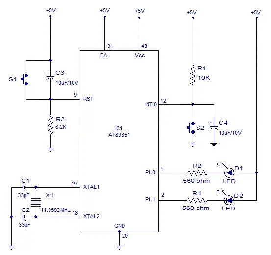
In the circuit shown above
D1, D2 (the LEDs to be toggled) are connected to P1.0 and P1.1
respectively. R2 and R4 limits the current through the LEDs. The push
button switch S2 is connected to the INT0 pin where R1 is a pull up
resistor and C4 is the debouncing capacitor. C3, R3 and S3 forms the
reset circuitry. Capacitors C2, C2 and crystal X1 are related to the
clock circuitry. When powered ON LED D1 will be OFF and and LED D2 will
be ON. Whenever push button switch S2 is pressed it creates an
interrupt and the software makes the status of P1.o and P1.1 to toggle
which gets reflected in the LEDs.
Program.
ORG 000H // starting address
SJMP LABEL //jumps to the LABEL
ORG 003H // starting address for the ISR(INT0)
ACALL ISR // calls the ISR (interrupt service routine)
RETI // returns from the interrupt
LABEL: MOV A,#10000000B // sets the initial stage of the LEDs (D1 OFF & D2 ON)
MAIN: // main function that sets the interrupt parameters
SETB IP.0 // sets highest priority for the interrupt INT0
SETB TCON.0 // interrupt generated by a falling edge signal at INT0 (pin12)
SETB IE.0 // enables the external interrupt
SETB IE.7 // enables the global interrupt control
SJMP MAIN // jumps back to the MAIN subroutine
ISR: // interrupt service routine
CPL A // complements the current value in accumulator A
MOV P1,A // moves the current accumulator value to port 1
RET // jumps to RETI
END
If you come across any doubts/errors while implementing this circuit, please feel free to ask in our comments section.


No comments:
Post a Comment