Tuesday, November 19, 2013

Low cost fire alarm circuit.

No comments:
Description.
When there is a fire breakout in the room the temperature increases. This ultra compact and low cost fire alarm senses fire breakout based on this fact.
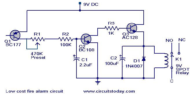
Transistor BC177 (Q1) is used as the fire sensor here. When the temperature increases the leakage current of this transistor also increases. The circuit is designed so that when there is an increase in the leakage current of Q1, transistor Q2 will get biased. As a result when there is a fire breakout the transistor Q2 will be on. The emitter of Q2 (BC 108) is connected to the base of Q3(AC 128). So when Q2 is ON Q3 will be also ON. The transistor Q3 drives the relay which is used to drive the load ie,light,bell,horn etc as an indication of the fire. The diode D1 is used as a free wheeling diode to protect it from back EMF generated when relay is switched.
Circuit diagram with Parts list.
fire-alarrm-circuit.JPG
Notes.
  • The Preset R1 can be used to desired temperature level for setting the alarm ON.
  • This is not a latching alarm,that is;when the temperature in the vicinity of the sensor decreases below the set point the alarm stops.
  • The circuit can be powered using  a 9V battery or a 9V battery eliminator.
  • All capacitors are electrolytic and must be rated at least 10V.
  • The load can be connected through the C,NC,NO points of the relay according to your need.
  • The calibration can be done using a soldering iron, and a thermo meter. Switch ON the power supply.Keep the tip of soldering iron near to the Q1. Same time also keep the thermometer close to it. When the temperature reaches your desired value adjust R1 so that relay gets ON.Done!
  • ---------------------------------------------------------------------------------------------------------------

Monday, November 18, 2013

100 Watt sub woofer amplifier.

2 comments:
Description.
This is the circuit diagram of a fully transistorized sub woofer amplifier that can produce an output of 100W.There are seven transistors including four in the output stage. The transistors Q1 and Q2 form the preamplifier stage. Transistors Q4 to Q7 form the output stage. Since no ICs are used the circuit is very robust and can be easily assembled on a general purpose PCB.
Circuit diagram with Parts list.
100-w-subwoofer-amplifier-circuit
Notes.
  • The circuit can be powered from a +35V/-35V, 5A dual power supply.
  • Use a 100W, 12 inch sub woofer at the output.
  • All electrolytic capacitors must be rated 100V.
  • The transistor Q4 to Q7 must be fitted with heat sinks.

-----------------------------------------------------------------------------------------------------

Working of Relays

No comments:

Working of Relays

In this article, the basics of a relay like energized relay and de-energized relay are explained in detail. Also, the design, construction, working, applications, and also relay selection is explained in detail.

What is a relay?

We know that most of the high end industrial application devices have relays for their effective working. Relays are simple switches which are operated both electrically and mechanically. Relays consist of a n electromagnet and also a set of contacts. The switching mechanism is carried out with the help of the electromagnet. There are also other operating principles for its working. But they differ according to their applications. Most of the devices have the application of relays.

Why is a relay used?

The main operation of a relay comes in places where only a low-power signal can be used to control a circuit. It is also used in places where only one signal can be used to control a lot of circuits. The application of relays started during the invention of telephones. They played an important role in switching calls in telephone exchanges. They were also used in long distance telegraphy. They were used to switch the signal coming from one source to another destination. After the invention of computers they were also used to perform Boolean and other logical operations. The high end applications of relays require high power to be driven by electric motors and so on. Such relays are called contactors.
TAKE A LOOK : TYPES OF RELAYS
TAKE A LOOK : HOW TO TEST A RELAY

Relay Design

There are only four main parts in a relay. They are
  • Electromagnet
  • Movable Armature
  • Switch point contacts
  • Spring
The figures given below show the actual design of a simple relay.
Relay Construction
Relay Construction
It is an electro-magnetic relay with a wire coil, surrounded by an iron core. A path of very low reluctance for the magnetic flux is provided for the movable armature and also the switch point contacts.  The movable armature is connected to the yoke which is mechanically connected to the switch point contacts. These parts are safely held with the help of a spring. The spring is used so as to produce an air gap in the circuit when the relay becomes de-energized.

How relay works?

The working of a relay can be better understood by explaining the following diagram given below.
Relay Design
Relay Design
The diagram shows an inner section diagram of a relay. An iron core is surrounded by a control coil. As shown, the power source is given to the electromagnet through a control switch and through contacts to the load. When current starts flowing through the control coil, the electromagnet starts energizing and thus intensifies the magnetic field. Thus the upper contact arm starts to be attracted to the lower fixed arm and thus closes the contacts causing a short circuit for the power to the load. On the other hand, if the relay was already de-energized when the contacts were closed, then the contact move oppositely and make an open circuit.
As soon as the coil current is off, the movable armature will be returned by a force back to its initial position. This force will be almost equal to half the strength of the magnetic force. This force is mainly provided by two factors. They are the spring and also gravity.
Relays are mainly made for two basic operations. One is low voltage application and the other is high voltage. For low voltage applications, more preference will be given to reduce the noise of the whole circuit. For high voltage applications, they are mainly designed to reduce a phenomenon called arcing.

Relay Basics

The basics for all the relays are the same. Take a look at a 4 – pin relay shown below. There are two colours shown. The green colour represents the control circuit and the red colour represents the load circuit. A small control coil is connected onto the control circuit. A switch is connected to the load. This switch is controlled by the coil in the control circuit. Now let us take the different steps that occour in a relay.
relay operation
relay operation
  • Energized Relay (ON)
As shown in the circuit, the current flowing through the coils represented by pins 1 and 3 causes a magnetic field to be aroused. This magnetic field causes the closing of the pins 2 and 4. Thus the switch plays an important role in the relay working. As it is a part of the load circuit, it is used to control an electrical circuit that is connected to it. Thus, when the relay in energized the current flow will be through the pins 2 and 4.
Energized Relay (ON)
  • De – Energized Relay (OFF)
As soon as the current flow stops through pins 1 and 3, the switch opens and thus the open circuit prevents the current flow through pins 2 and 4. Thus the relay becomes de-energized and thus in off position.
De-Energized Relay (OFF)
In simple, when a voltage is applied to pin 1, the electromagnet activates, causing a magnetic field to be developed, which goes on to close the pins 2 and 4 causing a closed circuit. When there is no voltage on pin 1, there will be no electromagnetic force and thus no magnetic field. Thus the switches remain open.

Pole and Throw

Relays have the exact working of a switch. So, the same concept is also applied. A relay is said to switch one or more poles. Each pole has contacts that can be thrown in mainly three ways. They are
  • Normally Open Contact (NO) – NO contact is also called a make contact. It closes the circuit when the relay is activated. It disconnects the circuit when the relay is inactive.
  • Normally Closed Contact (NC) – NC contact is also known as break contact. This is opposite to the NO contact. When the relay is activated, the circuit disconnects. When the relay is deactivated, the circuit connects.
  • Change-over (CO) / Double-throw (DT) Contacts – This type of contacts are used to control two types of circuits. They are used to control a NO contact and also a NC contact with a common terminal. According to their type they are called by the names break before make and make before breakcontacts.
Relays are also named with designations like
  • Single Pole Single Throw (SPST) – This type of relay has a total of four terminals. Out of these two terminals can be connected or disconnected. The other two terminals are needed for the coil.
  • Single Pole Double Throw (SPDT) – This type of a relay has a total of five terminals. Out f these two are the coil terminals. A common terminal is also included which connects to either of two others.
  • Double Pole Single Throw (DPST) – This relay has a total of six terminals. These terminals are further divided into two pairs. Thus they can act as two SPST’s which are actuated by a single coil. Out of the six terminals two of them are coil terminals.
  • Double Pole Double Throw (DPDT) – This is the biggest of all. It has mainly eight relay terminals. Out of these two rows are designed to be change over terminals. They are designed to act as two SPDT relays which are actuated by a single coil.

Relay Applications

  • Relays are used to realize logic functions. They play a very important role in providing safety critical logic.
  • Relays are used to provide time delay functions. They are used to time the delay open and delay close of contacts.
  • Relays are used to control high voltage circuits with the help of low voltage signals. Similarly they are used to control high current circuits with the help of low current signals.
  • They are also used as protective relays. By this function all the faults during transmission and reception can be detected and isolated.

Relay Selection

You must note some factors while selecting a particular relay. They are
  • Protection – Different protections like contact protection and coil protection must be noted. Contact protection helps in reducing arcing in circuits using inductors.  Coil protection helps in reducing surge voltage produced during switching.
  • Look for a standard relay with all regulatory approvals.
  • Switching time – Ask for high speed switching relays if you want one.
  • Ratings – There are current as well as voltage ratings. The current ratings vary from a few amperes to about 3000 amperes.  In case of voltage ratings, they vary from 300 Volt AC to 600 Volt AC. There are also high voltage relays of about 15,000 Volts.
  • Type of contact used – Whether it is a NC or NO or closed contact.
  • Select Make before Break or Break before Make contacts wisely.
  • Isolation between coil circuit and contacts
----------------------------------------------------------------------------------

Simple UPS

No comments:
Description.
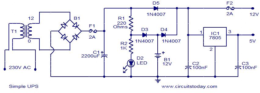
This is the circuit diagram of a simple UPS that can deliver 12V unregulated and 5V regulated DC. The transformer T1 steps down the mains voltage to 12V AC and then the bridge B1 rectifies it. The rectified signal is smoothed by the capacitor C1.When the mains supply is available the battery will be charged via diode D3 and the regulator IC gets supply via diode D5. 12V and 5V DC will be available at the output terminals. When mains supply is not available the battery supplies current to the regulator IC and to the 12V DC terminal through diode D4.Also, the diode D3 blocks reverse flow of current during battery mode. Capacitors C2 and C3 acts as filters.
Circuit diagram with Parts list.
simple-ups-circuit
Notes.
  • Assemble the circuit on a good quality PCB.
  • The transformer T1 can be a 230V AC primary, 12V secondary,3A step-down transformer.
  • The bridge B1 can be a 2A bridge. If such a bridge is not available, make one using four 1N4007 diodes.
  • The capacitor C1 must be rated at least 25V.


******Related Topic ******


Interfacing dot matrix LED display to 8051

No comments:

Interfacing dot matrix LED display to 8051 microcontroller.

LED dot matrix display.
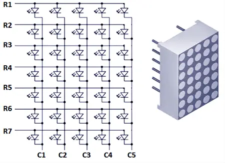
An LED dot matrix display consists of a matrix of  LED’s arranged in a rectangular configuration. The desired character or graphics can be displayed by switching ON /OFF  a desired configuration of LED’s. Common display configurations available are 7×5, 8×8, 7×15, etc. LED dot matrix can be used in simple display applications where the resolution is not a big concern.  The figure below shows the arrangement of LEDs in a typical 7×5 dot matrix display.

7x5 led dot matrix display
7x5 Led dot matrix display
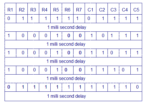
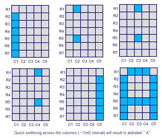
Any individual LED or a group of LEDs in the matrix can be activated by switching the required number of rows and columns. For example, in the above figure if  Row1 is made high and Column1 is made low, the top left LED (address R1C1) will glow. As a demonstration, lets see how we can display letter “A” using the display. The tables given below shows the logic levels at each pin  for displaying A.
led dot matrix displaydot matrix led display
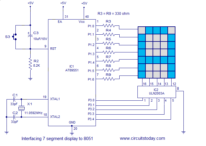
In the above diagram you can see that only one LED in a row will be ON at a time but any number of  LEDs in a column can be ON at a time.  That means the microcontroller’s port pin can directly drive a row but it requires  additional circuit for driving the column lines.  The circuit diagram for interfacing dot matrix display and 8051 microcontroller is shown below.
Circuit diagram.
interfacing dot matrix led display to 8051
ULN2003A driver IC.
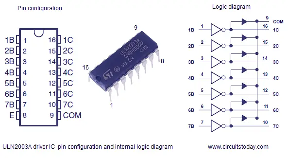
The purpose of ULN2003A here is to drive the column lines of the display. ULN2003A is a high voltage (50V), high current (500mA per channel) darlington transistor array. Each IC has 7 channels with individual output clamp diodes. ULN2003A  an active high device, which means a logic high must be applied to the input  to make the corresponding output high. The input pins are designated as 1B, 2B, 3B, 4B, 5B, 6B, 7B while corresponding output pins are designated as 1C, 2C, 3C, 4C, 5C, 6C, 7C.  The pin configuration and simplified internal logic of ULN2003A is shown in the figure below.
uln2003 logic diagram
Program.
ORG 00H
MOV P3,#00000000B        // initializes port 3 as output port
MOV P1,#00000000B        // initializes port 1 as output port
MAIN: MOV P3,#01111110B
      MOV P1,#11111110B
      ACALL DELAY
      MOV P3,#00010001B
      MOV P1,#11111101B
      ACALL DELAY
      MOV P3,#00010001B
      MOV P1,#11111011B
      ACALL DELAY
      MOV P3,#00010001B
      MOV P1,#11110111B
      ACALL DELAY
      MOV P3,#01111110B
      MOV P1,#11101111B
      ACALL DELAY
      SJMP MAIN         // jumps back to the main loop
DELAY: MOV R6,#255D     // 1ms delay subroutine
HERE: DJNZ R6,HERE
      RET
END
 --------------------------------------------------------------------------------------------------------------

Sunday, November 17, 2013

Build Your Own Arduino Board

5 comments:


Need more Arduino board? Do not spend more money for another one. Why not try to build your own DIY Arduino board? It is easy and simple.


atmega328p


                                                            atmega328p


DIY Arduino Step 1
Get an Atmega328–PU or Atmega328P-PU (with bootloader inside).
A brief introduction on the Atmega328 chip:
  • 8-bit MCU
  • 32kB Flash Memory
  • 1kB EEPROM
  • 2kB SRAM
  • 23 general purpose IO lines
  • 6-channel 10 bit ADC
  • SPI and I2C capabilities
Make Your Arduino Step 2
Connect the circuit as below:


arduino breadboard schematic


TAKE NOTE
In this post, I will talk about uploading sketches using FTDI programming port. In the next post, I will talk more about uploading sketches and burning bootloader using the ICSP programming port. Get one FTDI programmer here.
Build Your Arduino Step 3
Using FTDI programmer:
Now I will address one of the issues of making your own Arduino. On the Uno boards, there’s an IC which is responsible as a USB to serial converter and it makes it possible to program the Arduino and also communicate with it from the computer.
The problem here is the IC is an SMD (Surface Mounted Device). The R3 uses an ATmega 16U2 while the older revisions uses the 8U2. So, we need an FTDI programmer for the purpose of uploading the code/sketch into the chip.
FTDI programmer
FTDI programmer
When you first plug in your FTDI programmer into your laptop, you have to install the driver file. Get the driver file here.
Once installed, just connect the FTDI programmer to the FTDI programming port of DIY Arduino accordingly.
Finally just click on upload to upload the code into the chip!
If you don’t have the extra 16 MHz crystal and 18-22 picofarad capacitors used in the above examples, you can configure the ATmega328 to use its internal 8 MHz RC oscillator as a clock source instead. You don’t really need the 10K pullup resistor on the reset pin either, so we remove it to get a truly minimal configuration.
You’ll need to install support for an additional hardware configuration:
  • Download this hardware configuration archive: breadboard.zip
  • Create a “hardware” sub-folder in your Arduino sketchbook folder (whose location you can find in the Arduino preferences dialog). If you’ve previously installed support for additional hardware configuration, you may already have a “hardware” folder in your sketchbook.
  • Move the “breadboard” folder from the zip archive to the “hardware” sub-folder of your Arduino sketchbook.
  • Restart the Arduino software.
  • You should see “ATmega328 on a breadboard (8 MHz internal clock)” in the Tools > Board menu.
Once you’ve done this, you can burn the bootloader and upload programs onto your ATmega328 as described above. Be sure to select “ATmega328 on a breadboard (8 MHz internal clock)” when burning the bootloader.
If you select the wrong item and configure the microcontroller to use an external clock, it won’t work unless you connect one.
Finally, you have success in making your own DIY Arduino, meaning that you can upload arduino coding into your chip!
VINduino on stripboard

------------------------------------------------------------------------------------------------------------


Arduino YUN Release Date Anyone?

No comments:
According to the official statement Arduino is preparing its new release YUN, the first member of a new line of wifi products combining the power Linux with ease of use of Arduino. The release date is not revealed but I bet will happen soon and am so excited about this news, probably will be one of their first buyers.
BTW does anyone knows when Arduino YUN will be released because I really want to start making some interesting Arduino projects with it?


Arduino YUN Specs

  • Microcontroller: ATmega32u4
  • Operating Voltage: 5V
  • Input Voltage: 5V via microUSB or PoE 802.3af
  • Input Voltage: 6-20V
  • Digital I/O Pins: 14
  • PWM Channels: 7
  • Analog Input Channels: 6 (plus 6 multiplexed on 6 digital pins)
  • DC Current per I/O Pin: 40 mA
  • DC Current for 3.3V Pin: 50 mA
  • Flash Memory: 32 KB (ATmega32u4) of which 4 KB used by bootloader
  • SRAM: 2.5 KB (ATmega32u4)
  • EEPROM: 1 KB (ATmega32u4)
  • Clock Speed: 16 MHz
  • Processor: MIPS 24K operating at up to 400 MHz
  • Memory: DDR2 64MB Ram and 16 MB SPI Flash
  • AP or router: Complete IEEE 802.11bgn 1×1
  • Host/Device: USB 2.0
  • MicroSD: PoE compatible 802.3af card support

Basic Types and pinout of Arduino

2 comments:

Arduino Uno Pinout


Arduino Uno R3 Pinouts

Input and Output
Each of the 14 digital pins on the Arduino Uno can be used as an input or output, using pinMode(), digitalWrite(), and digitalRead() functions. They operate at 5 volts. Each pin can provide or receive a maximum of 40 mA and has an internal pull-up resistor (disconnected by default) of 20-50 kOhms.
In addition, some pins have specialized functions:

Serial: pins 0 (RX) and 1 (TX). Used to receive (RX) and transmit (TX) TTL serial data. These pins are connected to the corresponding pins of the ATmega8U2 USB-to-TTL Serial chip.
External Interrupts: pins 2 and 3. These pins can be configured to trigger an interrupt on a low value, a rising or falling edge, or a change in value. See the attachInterrupt() function for details.
PWM: 3, 5, 6, 9, 10, and 11. Provide 8-bit PWM output with the analogWrite() function.
SPI: 10 (SS), 11 (MOSI), 12 (MISO), 13 (SCK). These pins support SPI communication using the SPI library.
LED: 13. There is a built-in LED connected to digital pin 13. When the pin is HIGH value, the LED is on, when the pin is LOW, it’s off.
The Uno has 6 analog inputs, labeled A0 through A5, each of which provide 10 bits of resolution (i.e. 1024 different values). By default they measure from ground to 5 volts, though is it possible to change the upper end of their range using the AREF pin and the analogReference() function. Additionally, some pins have specialized functionality:
TWI: A4 or SDA pin and A5 or SCL pin. Support TWI communication using the Wire library.
There are a couple of other pins on the board:
AREF. Reference voltage for the analog inputs. Used with analogReference().
Reset. Bring this line LOW to reset the microcontroller. Typically used to add a reset button to shields which block the one on the board.

Arduino Leonardo Pinout


arduino leonardo pinout


Input and Output
Each of the 20 digital i/o pins on the Arduino Leonardo can be used as an input or output, using pinMode(), digitalWrite(), and digitalRead() functions. They operate at 5 volts. Each pin can provide or receive a maximum of 40 mA and has an internal pull-up resistor (disconnected by default) of 20-50 kOhms.
In addition, some pins have specialized functions:

Serial: 0 (RX) and 1 (TX). Used to receive (RX) and transmit (TX) TTL serial data using the ATmega32U4 hardware serial capability. Note that on the Leonardo, the Serial class refers to USB (CDC) communication; for TTL serial on pins 0 and 1, use the Serial1 class.
TWI: 2 (SDA) and 3 (SCL). Support TWI communication using the Wire library.
External Interrupts: 2 and 3. These pins can be configured to trigger an interrupt on a low value, a rising or falling edge, or a change in value. See the attachInterrupt() function for details.
PWM: 3, 5, 6, 9, 10, 11, and 13. Provide 8-bit PWM output with the analogWrite() function.
SPI: on the ICSP header. These pins support SPI communication using the SPI library. Note that the SPI pins are not connected to any of the digital I/O pins as they are on the Uno, They are only available on the ICSP connector. This means that if you have a shield that uses SPI, but does NOT have a 6-pin ICSP connector that connects to the Leonardo’s 6-pin ICSP header, the shield will not work.
LED: 13. There is a built-in LED connected to digital pin 13. When the pin is HIGH value, the LED is on, when the pin is LOW, it’s off.
Analog Inputs: A0-A5, A6 – A11 (on digital pins 4, 6, 8, 9, 10, and 12). The Leonardo has 12 analog inputs, labeled A0 through A11, all of which can also be used as digital i/o. Pins A0-A5 appear in the same locations as on the Uno; inputs A6-A11 are on digital i/o pins 4, 6, 8, 9, 10, and 12 respectively. Each analog input provide 10 bits of resolution (i.e. 1024 different values). By default the analog inputs measure from ground to 5 volts, though is it possible to change the upper end of their range using the AREF pin and the analogReference() function.
There are a couple of other pins on the board:
AREF. Reference voltage for the analog inputs. Used with analogReference().
Reset. Bring this line LOW to reset the microcontroller. Typically used to add a reset button to shields which block the one on the board.


Arduino Mega 2560 Pinout


Arduino Mega 2560 Pinout


Input and Output
Each of the 54 digital pins on the Arduino 2560 Mega can be used as an input or output, using pinMode(), digitalWrite(), and digitalRead() functions. They operate at 5 volts. Each pin can provide or receive a maximum of 40 mA and has an internal pull-up resistor (disconnected by default) of 20-50 kOhms.
In addition, some pins have specialized functions:

Serial: 0 (RX) and 1 (TX);
Serial 1: 19 (RX) and 18 (TX);
Serial 2: 17 (RX) and 16 (TX);
Serial 3: 15 (RX) and 14 (TX).
Used to receive (RX) and transmit (TX) TTL serial data. Pins 0 and 1 are also connected to the corresponding pins of the ATmega16U2 USB-to-TTL Serial chip.
External Interrupts: 2 (interrupt 0), 3 (interrupt 1), 18 (interrupt 5), 19 (interrupt 4), 20 (interrupt 3), and 21 (interrupt 2). These pins can be configured to trigger an interrupt on a low value, a rising or falling edge, or a change in value. See the attachInterrupt() function for details.
PWM: 2 to 13 and 44 to 46. Provide 8-bit PWM output with the analogWrite() function.
SPI: 50 (MISO), 51 (MOSI), 52 (SCK), 53 (SS). These pins support SPI communication using the SPI library. The SPI pins are also broken out on the ICSP header, which is physically compatible with the Uno, Duemilanove and Diecimila.
LED: 13. There is a built-in LED connected to digital pin 13. When the pin is HIGH value, the LED is on, when the pin is LOW, it’s off.
TWI: 20 (SDA) and 21 (SCL). Support TWI communication using the Wire library. Note that these pins are not in the same location as the TWI pins on the Duemilanove or Diecimila.
The Mega2560 has 16 analog inputs, each of which provide 10 bits of resolution (i.e. 1024 different values). By default they measure from ground to 5 volts, though is it possible to change the upper end of their range using the AREF pin and analogReference() function.
There are a couple of other pins on the board:
AREF. Reference voltage for the analog inputs. Used with analogReference().
Reset. Bring this line LOW to reset the microcontroller. Typically used to add a reset button to shields which block the one on the board.


Arduino Mega ADK Pinout


Arduino Mega ADK Pinout


 Input and Output
Each of the 50 digital pins on the Arduino Mega ADK can be used as an input or output, using pinMode(), digitalWrite(), and digitalRead() functions. They operate at 5 volts. Each pin can provide or receive a maximum of 40 mA and has an internal pull-up resistor (disconnected by default) of 20-50 kOhms.
In addition, some pins have specialized functions:

Serial: 0 (RX) and 1 (TX);
Serial 1: 19 (RX) and 18 (TX);
Serial 2: 17 (RX) and 16 (TX);
Serial 3: 15 (RX) and 14 (TX).
Used to receive (RX) and transmit (TX) TTL serial data. Pins 0 and 1 are also connected to the corresponding pins of the ATmega8U2 USB-to-TTL Serial chip.
External Interrupts: 2 (interrupt 0), 3 (interrupt 1), 18 (interrupt 5), 19 (interrupt 4), 20 (interrupt 3), and 21 (interrupt 2). These pins can be configured to trigger an interrupt on a low value, a rising or falling edge, or a change in value. See the attachInterrupt() function for details.
PWM: 2 to 13 and 44 to 46. Provide 8-bit PWM output with the analogWrite() function.
SPI: 50 (MISO), 51 (MOSI), 52 (SCK), 53 (SS). These pins support SPI communication using the SPI library. The SPI pins are also broken out on the ICSP header, which is physically compatible with the Uno, Duemilanove and Diecimila.
USB Host: MAX3421E. The MAX3421E comunicate with Arduino with the SPI bus. So it uses the following pins:
Digital: 7 (RST), 50 (MISO), 51 (MOSI), 52 (SCK).
NB: Please do not use Digital pin 7 as input or output because is used in the comunication with MAX3421E
Non broken out on headers: PJ3 (GP_MAX), PJ6 (INT_MAX), PH7 (SS).
LED: 13. There is a built-in LED connected to digital pin 13. When the pin is HIGH value, the LED is on, when the pin is LOW, it’s off.
TWI: 20 (SDA) and 21 (SCL). Support TWI communication using the Wire library. Note that these pins are not in the same location as the TWI pins on the Duemilanove or Diecimila.
The ADK has 16 analog inputs, each of which provide 10 bits of resolution (i.e. 1024 different values). By default they measure from ground to 5 volts, though is it possible to change the upper end of their range using the AREF pin and analogReference() function.
There are a couple of other pins on the board:
AREF. Reference voltage for the analog inputs. Used with analogReference().
Reset. Bring this line LOW to reset the microcontroller. Typically used to add a reset button to shields which block the one on the board.

Arduino Ethernet Pinout


Arduino Ethernet Pinout


 Input and Output
Each of the 14 digital pins on the Ethernet board can be used as an input or output, using pinMode(), digitalWrite(), and digitalRead() functions. They operate at 5 volts. Each pin can provide or receive a maximum of 40 mA and has an internal pull-up resistor (disconnected by default) of 20-50 kOhms.
In addition, some pins have specialized functions:

Serial: 0 (RX) and 1 (TX). Used to receive (RX) and transmit (TX) TTL serial data.
External Interrupts: 2 and 3. These pins can be configured to trigger an interrupt on a low value, a rising or falling edge, or a change in value. See the attachInterrupt() function for details.
PWM: 3, 5, 6, 9, and 10. Provide 8-bit PWM output with the analogWrite() function.
SPI: 10 (SS), 11 (MOSI), 12 (MISO), 13 (SCK). These pins support SPI communication using the SPI library.
LED: 9. There is a built-in LED connected to digital pin 9. When the pin is HIGH value, the LED is on, when the pin is LOW, it’s off. On most other arduino boards, this LED is found on pin 13. It is on pin 9 on the Ethernet board because pin 13 is used as part of the SPI connection.
The Ethernet board has 6 analog inputs, labeled A0 through A5, each of which provide 10 bits of resolution (i.e. 1024 different values). By default they measure from ground to 5 volts, though is it possible to change the upper end of their range using the AREF pin and the analogReference() function. Additionally, some pins have specialized functionality:
TWI: A4 (SDA) and A5 (SCL). Support TWI communication using the Wire library.
There are a couple of other pins on the board:
AREF. Reference voltage for the analog inputs. Used with analogReference().
Reset. Bring this line LOW to reset the microcontroller. Typically used to add a reset button to shields which block the one on the board.


Arduino Due Pinout


Arduino Due Pinout


Input and Output
Digital I/O: pins from 0 to 53
Each of the 54 digital pins on the Due can be used as an input or output, using pinMode(), digitalWrite(), and digitalRead() functions. They operate at 3.3 volts. Each pin can provide (source) a current of 3 mA or 15 mA, depending on the pin, or receive (sink) a current of 6 mA or 9 mA, depending on the pin. They also have an internal pull-up resistor (disconnected by default) of 100 KOhm.
In addition, some pins have specialized functions:

Serial: 0 (RX) and 1 (TX)
Serial 1: 19 (RX) and 18 (TX)
Serial 2: 17 (RX) and 16 (TX)
Serial 3: 15 (RX) and 14 (TX)
Used to receive (RX) and transmit (TX) TTL serial data (with 3.3 V level). Pins 0 and 1 are connected to the corresponding pins of the ATmega16U2 USB-to-TTL Serial chip.
PWM: Pins 2 to 13
Provide 8-bit PWM output with the analogWrite() function. the resolution of the PWM can be changed with the analogWriteResolution() function.
SPI: SPI header (ICSP header on other Arduino boards)
These pins support SPI communication using the SPI library. The SPI pins are broken out on the central 6-pin header, which is physically compatible with the Uno, Leonardo and Mega2560. The SPI header can be used only to communicate with other SPI devices, not for programming the SAM3X with the In-Circuit-Serial-Programming technique. The SPI of the Due has also advanced features that can be used with the Extended SPI methods for Due.
CAN: CANRX and CANTX
These pins support the CAN communication protocol but are not not yet supported by Arduino APIs.
“L” LED: 13
There is a built-in LED connected to digital pin 13. When the pin is HIGH, the LED is on, when the pin is LOW, it’s off. It is also possible to dim the LED because the digital pin 13 is also a PWM outuput.
TWI 1: 20 (SDA) and 21 (SCL)
TWI 2: SDA1 and SCL1.
Support TWI communication using the Wire library.
Analog Inputs: pins from A0 to A11
The Due has 12 analog inputs, each of which can provide 12 bits of resolution (i.e. 4096 different values). By default, the resolution of the readings is set at 10 bits, for compatibility with other Arduino boards. It is possible to change the resolution of the ADC with analogReadResolution(). The Due’s analog inputs pins measure from ground to a maximum value of 3.3V. Applying more then 3.3V on the Due’s pins will damage the SAM3X chip. The analogReference() function is ignored on the Due.
The AREF pin is connected to the SAM3X analog reference pin through a resistor bridge. To use the AREF pin, resistor BR1 must be desoldered from the PCB.
DAC1 and DAC2
These pins provides true analog outputs with 12-bits resolution (4096 levels) with the analogWrite() function. These pins can be used to create an audio output using the Audio library.
Other pins on the board:
AREF
Reference voltage for the analog inputs. Used with analogReference().
Reset
Bring this line LOW to reset the microcontroller. Typically used to add a reset button to shields which block the one on the board.

--------------------------------------------------------------------------------------------------------------