Monday, November 11, 2013

Simple Transistor Type and Lead Identifier

2 comments:
A bipolar junction transistor (BJT) has three regions, of which the emitter and the collector are made of the same type of semiconductor (‘n’ for npn and ‘p’ for pnp) but the base is of opposite type. If we consider the base and emitter terminals (or the base and collector terminals), we get a p-n junction diode. But if we hold collector and emitter terminals, we encounter two diodes connected back-to-back.

On forward biasing the p-n junction (with a battery and a current-limiting resistor), the diode starts conducting and the drop of voltage across it is very small (0.7 volt for Si). On reverse biasing, the diode stops conducting and the drop of voltage across it is very close to the supply voltage. But, practically no current will flow through the collector and emitter terminals when we make the collector positive with respect to the emitter or vice versa.
This is the basis of the first part of our experiment that helps determine the type of a given transistor (whether npn or pnp) as also its base. But we cannot distinguish between the collector and the emitter in this way. To do so, we have to understand another basic principle.

BJTs have an intrinsic property of current amplification. While operating in the active region, a small current injected into the base can produce a large current flowing between the collector and emitter. The ratio of the collector current to the base current is known as forward current gain βF.

Although the collector and the emitter are made of the same type of semiconductor, we cannot expect a large current gain if we treat the collector as the emitter and the emitter as the collector.

If we forward bias the collector-base junction and reverse bias the base-emitter junction, we call it the inverse mode of operation. Because of the structural difference and doping levels, inverse current gain βI is exceedingly small. Thus while βF can be of the order of hundreds, βI is of the order of a few units only. This principle will be utilised in the second part of our experiment to distinguish between the collector and the emitter leads.

At the heart of the circuit (shown in Fig. 1) is a comparator built around operational amplifier IC 741 (IC1). With the help of a divider network comprising R3 and R4 between the positive supply terminal and ground, the inverting terminal is kept at reference voltage Vref=VssR4/(R3+R4) or –VssR4/(R3+R4) depending upon the selection of contact +Vss (marked ‘npn’) or –Vss (marked ‘npn’) by SPDT switch S1. The voltage at the non-inverting terminal is taken from the bottom end of resistor R2 (1-kilo-ohm) marked V+.
If V+>Vref, the comparator output will be high (positive saturation state ≈ +Vss) and the red LED will glow. On the other hand, if V+<Vref,the comparator output will be low(negative saturation state ≈ –Vss) andthe green LED will glow. The transi-tion from one state to the other is verymuch abrupt and under no circum-stances can both LEDs be ‘on’ or ‘off.’

The first part of the experiment for determination of the transistor type may be carried out as follows:
1. Label the terminals of the transistor under test (TUT) as 1, 2 and 3 arbitrarily.
2. Keeping aside socket C, use only sockets A and B in this part of the experiment.
3. Select the contact marked ‘n-p-n.’ This makes the voltage at socket A positive with respect to socket B (GND).
4. Take any pair of terminals of the transistor and insert one terminal in socket A and the other in socket B. Observe which LED turns on and which remains ‘off’ and record it.
5. Next, interchange the terminals in the two sockets and again observe the status of the LEDs and record it.
6. Repeat steps 4 and 5 for the remaining two pairs and record all the six observations in the form of a table.

From Table I, first find out the pair of terminals for which only the red LED glows even when the terminals are interchanged. These are the collector and emitter terminals. You cannot, however, detect which one of these would be the collector or the emitter from this part of experiment.

Once you have separated the collector and the emitter leads, the remaining lead will obviously be the base of the transistor.

Right up to this point, we do not know whether the transistor is npn- or pnp-type, because the assertion made above will remain valid for the collector and the emitter both being either ‘n’ type or ‘p’ type. The only thing we know is that the base will be of opposite-type semiconductor.

Since we know the polarity of ‘A’ (positive w.r.t. ‘B’), we search from Table I which LED was glowing when the base was put in socket A and any one of the other two leads in socket B.

If the green LED was glowing the base is p-type and the transistor is npn-type, but if the red LED was glowing the base is n-type and the transistor is pnp-type.

A typical record is shown in Table I, from which we find that the transistor is npn-type and lead 2 is the base. But, lead 1 or lead 3 could be the emitter or vice versa.

To detect the collector and the emitter, proceed as follows:
7. If the transistor is npn-type, set the pole of switch S1 towards ‘npn’ marking. If the transistor is pnp-type, set the pole of switch S1 towards ‘pnp’ marking.
8. Next, insert the base lead in socket C, any one of the remaining two leads in socket A and the rest in socket B. Observe as before the status of the two LEDs.

For an npn-type transistor, if the green LED glows the lead inserted in socket A will be collector, but if the red LED glows it will be emitter.

On the other hand, for a pnp-type transistor, if the green LED glows the lead inserted in socket A will be emitter, but if the red LED glows the reverse will be the case, i.e., the lead will be collector.

The status of the LEDs for the above-mentioned npn-type transistor having lead 2 as base is shown in Table II. From this table, we find that lead 1 is collector and lead 3 is emitter of the transistor in the example.


Electronics Lab   created by Muhammad Irfan  
Electronics Lab   created by Muhammad Irfan 

How to use a relay

No comments:
A relay is an electrically operated switch. Current flowing through the coil of the relay creates a magnetic field which attracts a lever and changes the switch contacts. The coil current can be on or off so relays have two switch positions and they are double throw (changeover) switches.
The relay’s switch connections are usually labeled COM(POLE), NC and NO:
COM/POLE= Common, NC and NO always connect to this, it is the moving part of the switch.
NC = Normally Closed, COM/POLE is connected to this when the relay coil is not magnetized.
NO = Normally Open, COM/POLE is connected to this when the relay coil is MAGNETIZED and vice versa.
A relay shown in the picture is an electromagnetic or mechanical relay.
  
Fig. Relay and its symbol
There are 5 Pins in a relay. Two pins A and B are two ends of a coil that are kept inside the relay. The coil is wound on a small rod that gets magnetized whenever current passes through it.
COM/POLE is always connected to NC(Normally connected) pin. As current is passed through the coil A, B, the pole gets connected to NO(Normally Open) pin of the relay.
Here is an example,
First of all try the following circuit.
This is a dark sensor circuit.
Output of this circuit: When you block light falling on LDR, the circuit switches on the LED- D1.
Now, replace LED-D1 and R2- 330R with a relay and diode.
Reconfigure the circuit as shown in the figure below:
Note: In R3, you can keep any resistor from 330R to 4.7K, this resistor is for sensitivity of the dark sensor.
The following circuit also works as a dark sensor. When you block light falling on LDR, the relay gets activated and Pole of relay gets connected to NO pin that eventually gives power to LED- D1.
 
Fig. Dark sensor using two transistors and a relay.

Light sensor using relay and transistors

In this case, the configuration of relay has been changed. Here, NO (Normally open) terminal has been left open. In normal case, the D1-LED remains ON. When light falling on LDR is interrupted, pole of relay gets connected to NO terminal. Hence, NC (Normally connected) terminal does not get power and that switches the D1- LED off.
Fig. Light sensor using two transistors and a relay.
Connect to COM(pole) and NO if you want the switched circuit to be on when the relay coil is on.
Connect to COM(pole) and NC if you want the switched circuit to be on when the relay coil is off.

WORKING WITH 220V

WARNING: IF YOU ARE A NOVICE DO NOT PLAY WITH 220V AC. CALL AN EXPERIENCED PERSON FOR ASSISTANCE.
Fig. Dark sensor circuit for 220V powered lights.
A relay can be used to turn on lights working on 220V, AC. The AC powered light has to be connected to relay as shown in the picture above.
Fig. Connecting wires on relay
The following video shows a soldered/finished prototype.

PROTECTION DIODE FOR RELAY

Fig. Protection diode in the circuit
Transistors and ICs must be protected from the brief high voltage produced when a relay coil is switched off. The diagram shows how a signal diode (eg 1N4148or 1N4001) is connected ‘backwards’ across the relay coil to provide this protection.
Current flowing through a relay coil creates a magnetic field which collapses suddenly when the current is switched off. The sudden collapse of the magnetic field induces a brief high voltage across the relay coil which is very likely to damage transistors and ICs. The protection diode allows the induced voltage to drive a brief current through the coil (and diode) so the magnetic field dies away quickly rather than instantly. This prevents the induced voltage becoming high enough to cause damage to transistors and ICs.

GENERAL SPECIFICATION OF A RELAY

06VDC- means that the voltage across the relay coil has to be 6V-DC.
50/60Hz- The relay can work under 50/60Hz AC.
7A, 240VAC- The maximum AC current and AC voltage specification that can be passed through NC, NO and pole pins/terminals of relay.

Experiments with 741- Operational amplifier

No comments:
Description: This versatile 741 operational amplifier module can be used for making a dark detector using an LDR, a photo transistor and a photo diode. The amplifier has been configured in inverting mode. It compares the change in voltage at pin 2 with the reference voltage at pin 3 and gives output at pin 6 accordingly. 


REQUIRED COMPONENTS: 
Project on mini breadbaord:
741-experiment>
dark-sensor-using-741-and-LDR1 title=
Schematic:
741-and-photo-transistor
-

Saturday, October 26, 2013

Simple Mobile Phone Jammer Circuit Diagram

1 comment:
Description
                 Circuit showing a mobile phone jammer.Here i have used a fm transistor for making this circuit.Mobile phones are working in 450  MHz  frequency .Here the transmitter generate almost equal to 450 MHz  frequency there for the mobile phone does not identify the original signal but the signal range is very week so this circuit working in only 100 m range .This circuit working in only 450 Mhz .Do not give more than 3 V


Part List
Component No: Value  Usage
R1 100R  Emitter loading
R2 39k   Base Biasing
C115 pf  Frequency
 Generating
C24.7pf  Feedback
C3 4.7pf  Feedback
C4102pf  Noise Reduce
C5 1MFCoupling
C6 2.2pf  Coupling
C7    103pf    Decoupling 
Q1 BF 494  Amplification
L1 22nH Frequency
 Generating

Applications

* FM Transmission

* TV Transmission

* Remote Controlled Toy


Electronics  lab   ,     Created by Muhammad Irfan

Wednesday, October 23, 2013

Water level controller using 8051

No comments:
A water level controller based using 8051 is shown in this article. A lot of water level controller projects have been published in this website but the is the first one based on a microcontroller. This water level controller monitors the level of the over head tank  and automatically switches on the water pump when ever the level goes below a preset limit. The level of the over head tank is indicated using 5 leds and the pump is switched of when the over head tank is filled. The pump is not allowed to start if the water level in the sump tank is low and also the pump is switched off when the level inside the sump tank goes low during a pumping cycle. The circuit diagram of the water level controller is shown below.
The level sensor probes for the overhead tank are interfaced to the port 2 of the microcontroller through transistors. Have a look at the sensor probe arrangement for the overhead tank in Fig1. A positive voltage supply probe goes to the down bottom of the tank. The probes for sensing 1/4, 1/2, 3/4 and FULL levels are placed with equal spacing one by one above the bottom positive probe. Consider the topmost (full level) probe, its other end is connected to the base of transistor Q4 through resistor R16. Whenever water rises to the full level current flows into the base of transistor Q4 which makes it ON and so its collector voltage goes low. The collector of Q4 is connected to P2.4 and a low voltage at  P2.4 means the over head tank is not FULL. When water level goes below the full level probe, the base of Q2 becomes open making it OFF. Now its collector voltage goes high and high at P2.4 means the tank is not full. The same applies to other sensor probes (3/4, 1/2, 1/4) and the microprocessor understands the current level by scanning the port pins P2.4 ,P2.5, P2.6 and P2.7. All these port pin are high (all sensor probes are open) means the tank is empty.
Port pin P0.5 is used to control the pump. When ever it is required start pumping, the controller makes P0.5 low which makes transistor Q6 ON which in turn activates the relay K1 that switches the pump. Also the LED d6 glows indicating the motor is ON. LED D7 is the low sump indicator. When the water level in the sump tank goes low, the controller makes P0.7 low which makes LED D7 to glow. The circuit diagram of the water level controller is shown in the figure below.


Circuit diagram.

Program.


MOV P2,#11111111B // initiates P2 as sensor input
MOV P0,#11111111B // initiates P2 as the output port
MOV A,#00000000B
MAIN:ACALL SMPCK // checks the level of the sump tank
MOV A,P2 // moves the current status of P2 tp A
CJNE A,#11110000B,LABEL1 // checks whether tank is full
SETB P0.1
SETB P0.2
SETB P0.3
SETB P0.4
CLR P0.0 // glows full level LED
SETB P0.5
LABEL1:MOV A,P2
CJNE A,#11111000B,LABEL2 // checks whether tank is 3/4
SETB P0.0
SETB P0.2
SETB P0.3
SETB P0.4
CLR P0.1 // glows 3/4 level LED
LABEL2:MOV A,P2
CJNE A,#11111100B,LABEL3 // checks whether tank is 1/2
SETB P0.0
SETB P0.1
SETB P0.3
SETB P0.4
CLR P0.2 // glows 1/2 level LED
LABEL3:MOV A,P2
CJNE A,#11111110B,LABEL4 // checks whether tank is 1/4
SETB P0.0
SETB P0.1
SETB P0.2
SETB P0.4
CLR P0.3 // glows 1/4 level LED
JB P0.6,LABEL4
CLR P0.5 // switches motor ON
LABEL4:MOV A,P2
CJNE A,#11111111B,MAIN // checks whether tank is empty
SETB P0.0
SETB P0.1
SETB P0.2
SETB P0.3
CLR P0.4 // glows EMPTY LED
JB P0.6,MAIN // checks whether sump is low
CLR P0.5 // switches motor ON
SJMP MAIN
SMPCK:JB P0.6,LABEL5 // checks whether sump is low
SETB P0.7 // extinguishes the sump low indicator LED
SJMP LABEL6
LABEL5:SETB P0.5 // switches the pump OFF
CLR P0.7 // glows sump low indicator LED
LABEL6:RET
END

 Electronics  lab   ,     Created by Muhammad Irfan 


Monday, October 21, 2013

Object counter using 8051

1 comment:

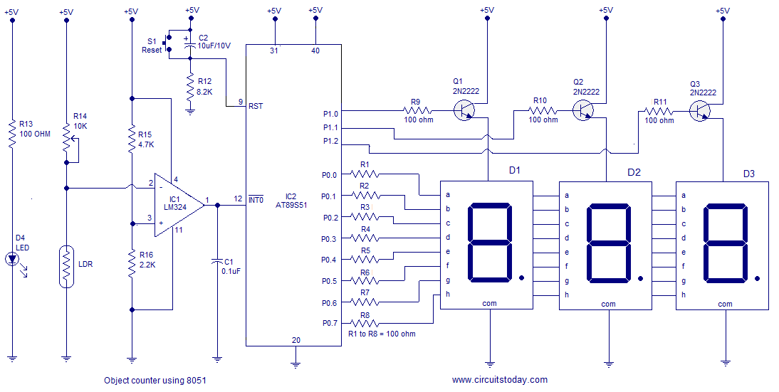
Object counter using 8051 microcontroller.

This article is about a simple object counter/visitor counter using 8051 microcontroller . AT89S51 belonging to the 8051 family is the microcontroller used here. This circuit can count the number of objects passing across a line , number of persons passing through a gate/door and so on. The can be simply divided into two sections i.e. the sensor section and the display section.

Sensor.                                                  

The sensor part consists of a ultra bright led (with focus), and LDR, opamp LM324 and the associated passive components. The LED is placed on one side of the door and the LDR is placed on the other side so that the light from the LED falls directly on the LDR.As you know, the resistance of the LDR has an inverse relationship with the intensity of the light falling on it. The preset resistor R14 is so adjusted that the voltage across the LDR is below 1.5V when it is illuminated. This voltage (labelled A in the circuit diagram) is connected to the inverting input of the opamp which is wired as a comparator with reference voltage 1.5V (set using R15 and R16).Capacitor C1 is meant for bypassing noise or anything like that which may cause false triggering.Resistor R13 is meant to control the current through the LED. 

Electronics  lab   ,     Created by Muhammad Irfan
When the light is falling on the LDR the voltage across it will be less than the reference voltage and so the output of the opamp remains high. When the light beam is interrupted, the voltage across the LDR goes above the reference voltage and so the opamp output goes low and it indicates a pass.

Display section.

The output of the opamp is fed to the INTO (interrupt 0) pin of the microcontroller. The microcontroller is programmed to count the number of negative edge pulses received at the INT0 pin and displays it on the three digit seven segment display.

Circuit diagram.


Program.

ORG 000H
SJMP INIT
ORG 003H  // starting address of interrupt service routine (ISR)
ACALL ISR // calls interrupt service routine
RETI

INIT: MOV P0,#00000000B
      MOV P3,#11111111B
      MOV P1,#00000000B
      MOV R6,#00000000B
      MOV DPTR,#LUT
      SETB IP.0     // sets highest priority for the interrupt INT0
      SETB TCON.0   // interrupt generated by a falling edge signal at INT0 pin
      SETB IE.0     //enables the external interrupt
      SETB IE.7     //enables the global interrupt control

MAIN: MOV A,R6
      MOV B,#100D
      DIV AB
      ACALL DISPLAY
      SETB P1.0
      ACALL DELAY
      ACALL DELAY
      MOV A,B
      MOV B,#10D
      DIV AB
      ACALL DISPLAY
      CLR P1.0
      SETB P1.1
      ACALL DELAY
      ACALL DELAY
      MOV A,B
      ACALL DISPLAY
      CLR P1.1
      SETB P1.2
      ACALL DELAY
      ACALL DELAY
      CLR P1.2
      SJMP MAIN

ISR: INC R6     //interrupt service routine
     RET

DISPLAY: MOVC A,@A+DPTR // display sub routine
         CPL A
         MOV P0,A
         RET

DELAY: MOV R3,#255D  // 1mS delay
LABEL: DJNZ R3,LABEL
       RET
LUT: DB 3FH
     DB 06H
     DB 5BH
     DB 4FH
     DB 66H
     DB 6DH
     DB 7DH
     DB 07H
     DB 7FH
     DB 6FH
END

About the program.

The program is written so that, it keeps displaying the current value in register R6 on the three digit seven segment display. When ever there is a valid negative going pulse (interrupt) at the INT0 pin, the program branches to the interrupt service routine (sub routine ISR). Subroutine ISR increments the value in register R6, then jumps back to the MAIN loop and the display gets updated by the new value.

Notes.

Entire circuit can be powered from a 5V DC supply.
LDR must be placed in an enclosure so that the light from LED alone falls on it.


Electronics  lab   ,     Created by Muhammad Irfan 


Automatic Doorbell with Object Detection Circuit

2 comments:

Automatic Doorbell with Object Detection Circuit


PROJECT SUMMARY

The circuit operates using a pair of ultrasonic transmitter and receiver modules which are used to detect the person. When the person is detected (the person is in the front door), the doorbell is automatically turned ON.

PROJECT DESCRIPTION


Figure 1  Automatic Door Bell with Object Detection Circuit Diagram


The ultrasonic transmitter operates at a frequency of about 40 kHz, which means it continuously transmits the ultrasonic waves of about 40 kHz. The power supplied should be moderate such that the range of the transmitter is only about one or two meters. If the transmitting power is less than one meter, then there is a possibility that the person who is one meter away will not be detected. Likewise, if the range is set higher, then it may lead to false trigerring which means that objects from afar maybe considered as visitors triggering the circuit. So to avoid these problems, the transmitting power is kept to an optimum level.
The ultrasonic receiver module receives the power with the frequency the same as that of the transmitter so that the noise will be eliminated and minimized false triggering. The sensitivity of the receiver can be tuned by using a 500 kilo-ohm variable resistor arranged as a pot in the circuit. By tuning this properly, we can achieve the desired results. The buzzer circuit is the output load which acts a doorbell in the case. The receiver circuit uses the integrated circuit LM324 which has 4 operational amplifier internally. Out of the four, three operational amplifiers only are being utilized. The three op-amps are arranged in cascade to provide high gain as well as noise free output.
An optocoupler is used at the output to avoid any interaction between the circuit and the doorbell.
Assemble the circuit on a PCB as compactly as possible and then attach it to the main door. You may provide a power supply using a 9 VDC adapter with filtered and regulated output. If the 9 V adapter with regulated output is not available, then we recommend you to use a 12 V unregulated DC adapter with 7809 voltage regulator.


Electronics  lab   ,     Created by Muhammad Irfan Electronics  lab   ,     Created by Muhammad Irfan


Resistance Calculator From Band

No comments:

Calculate the resistance of a 4 band resistor


Introduction

A resistor is a perhaps the most common building block used in circuits. Resistors come in many shapes and sizes this tool is used to decode information for color banded axial lead resistors.

4 Band Description

The number of bands is important because the decoding changes based upon the number of color bands. There are three common types: 4 band, 5 band, and 6 band resistors. For the 4 band resistor:
Band 1 – First significant digit.
Band 2 – Second significant digit
Band 3 – Multiplier
Band 4 – Tolerance

Resistance Value

The first 4 bands make up the resistance nominal value. The first 2 bands make up the significant digits where:
black – 0
brown – 1
red – 2
orange – 3
yellow – 4
green – 5
blue – 6
violet – 7
grey – 8
white – 9
The 3rd band or multiplier band is color coded as follows:
black – x1
brown – x10
red – x100
orange – x1K
yellow – x10K
green – x100K
blue – x1M
violet – x10M
grey – x100M
white – x1G
gold – .1
silver – .01
An example of a resistance value is:
band 1 = orange = 3,
band 2 = yellow = 4,
band 3 = blue = 1M
value = 34*1M = 34 Mohm

Resistance Tolerance

The fourth band is the tolerance and represents the worst case variation one might expect from the nominal value. The color code for tolerance is as follows:
brown – 1%
red – 2%
orange – 3%
yellow – 4%
green – .5%
blue – .25%
violet – .1%
gray – .05%
gold – 5%
silver – 10%
An example calculating the range of a resistor value is:
If the nominal value was 345 Ohm and the 4th band of the resistor was gold (5%) the value range would be nominal +/- 5% = 32.3 to 35.7

Also Over Here 


Electronics  lab   ,     Created by Muhammad Irfan 
Electronics  lab   ,     Created by Muhammad Irfan
Advertisement
Advertisement
 WEBENCH® Designer

    Enter your power supply requirements:
    DC  AC

    Vin
    Min
    VMax
    V
    OutputVout
    VIout
    A
    Ambient Temp°C
    Multiple Loads
    Single Output